Introduction to Programmable Logic
280 likes | 310 Vues
Dive into the realm of programmable logic devices with this comprehensive guide covering basics, architecture, design flow, and industry trends. Explore digital logic functions, field-programmable gate arrays (FPGAs), ASICs, and FPGA architecture in detail.

Introduction to Programmable Logic
E N D
Presentation Transcript
Introduction toProgrammable Logic John Coughlan RAL Technology Department Electronics Division
PPD Lectures • Data Transport • Triggering • Computers interacting with Hardware (VME Bus) • Silicon Trackers (Millions of Data Channels) • Programmable Logic is Key Underlying Technology. • Commercial Devices. Driven by Industry.
Particle Physics Electronics CMS Custom Electronics Chips Radn Hard, Low Power CERN LHC Electronics “Counting” Room(s) Trigger Systems. DAQ Systems. Purpose Built Digital Processing Boards In VME Bus Crates
Particle Physics Electronics • Special Dedicated Logic Functions (not possible in CPUs) • Ultra Fast Trigger Systems (Trigger Algorithms) Clock Accurate Timing • Massively Parallel Data Processing (Silicon Trackers with Millions of Channels) Custom Designed Printed Circuit Boards PCBs. Commercial Programmable Logic Devices
Lecture Outline • Programmable Logic Devices • Basics • Evolution • Field Programmable Gate Arrays (FPGAs) • Architecture • Design Flow • Design Tools • Hardware Description Languages • Industry Trends
Digital Logic Digital Logic Function Product AND (&) Sum OR (|) 3 Inputs SUM of PRODUCTS Black Box Truth Table Boolean Logic Minimisation Connect Standard Logic Chips Very Simple Glue Logic FIXED Logic Transistor Switches
Programmable Logic Devices PLDs • Different Types • SUM of PRODUCTS • Prefabricated • Programmble Links • Reconfigurable Un-programmed State Planes of ANDs, ORs Logic Function Inputs Sums ANDs OR Programmed PLD Product Terms Sum of Products
Feedback Outputs CPLD Architecture Complex PLDs • CPLDs • Programmable PLD Blocks • Programmable Interconnects • Electrically Erasable links
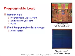
Application Specific Integrated Circuits ASICs Prefabricated Programmed Custom Fabricated Design from Scratch Large Complex Functions . Millions of Gates Customised for Extremes of Speed, Low Power, Radiation Hard (Very) Expensive (in small quantities) > $1 Million mask set (Very) Hard to Design. Long Design cycles. NOT Reprogrammable. High Risk Limited Complexity Thousands of Gates Cheap Easy to Design Reprogrammable.
Application Specific Integrated Circuits ASICs FPGA Large Complex Functions Inexpensive Easy to Design Reprogrammable.
Field Programmable Gate Arrays FPGA • Field Programmable Gate Array • New Architecture • ‘Simple’ Programmable Logic Blocks • Massive Fabric of Programmable Interconnects Large Number of Logic Block ‘Islands’ 1,000 … 100,000+ in a ‘Sea’ of Interconnects FPGA Architecture
Logic Blocks • Logic Functions implemented in Lookup Table LUTs • Multiplexers (select 1 of N inputs) • Flip-Flops. Registers. Clocked Storage elements. FPGA Fabric Logic Block
Lookup Tables LUTs • LUT contains Memory Cells to implement small logic functions • Each cell holds ‘0’ or ‘1’ . • Programmed with outputs of Truth Table • Inputs select content of one of the cells as output 3 Inputs LUT -> 8 Memory Cells 3 – 6 Inputs Static Random Access Memory SRAM cells Multiplexer MUX
Logic Blocks • Larger Logic Functions built up by connecting many Logic Blocks together
Clocked Logic • Flip Flops on outputs. CLOCKED storage elements. • Sequential Logic Functions (cf Combinational Logic LUTs) • Pipelines. Synchronous Logic Design • FPGA Fabric driven by Global Clock (e.g. BX frequency) FPGA Fabric Clock
FPGA Design Synchronous Logic • Pipelining Logic • Combinational Logic Result
FPGA Design Synchronous Logic • Pipelining Logic • Combinational Logic Stored in Registers. • Clocked Logic (e.g. at LHC BX 40 MHz) Once Pipeline Full New Result every Clock Period
FPGA Design Synchronous Logic • Pipelining • Combinational and Sequential Logic. • Clocked Logic (e.g. at LHC BX 40 MHz)
Clocked Logic • FPGA Fabric driven by Global Clock (e.g. BX frequency) Register Transfer Logic RTL FPGA Fabric Clock
Routing • Connections Routing signals between Logic Blocks • Determined by SRAM cells Special Routing for Clocks Around Fabric Edges Configurable Input Output I/O Blocks 100’s – 1,000 Pins
Configuring an FPGA • Millions of SRAM cells holding LUTs and Interconnect Routing • Volatile Memory. Loses configuration when board power is turned off. • Keep Bit Pattern describing the SRAM cells in non-Volatile Memory e.g. ROM or Digital Camera card • Configuration takes ~ secs JTAG Port Programming Bit File JTAG Testing
Designing Logic with FPGAs • High level Description of Logic Design • Hardware Description Language (Textual) • Compile (Synthesise) into Netlist. • Boolean Logic Gates. • Target FPGA Fabric • Mapping • Routing • Bit File for FPGA • Commercial CAE Tools (Complex & Expensive) • Logic Simulation Design Flow
Hardware Description Languages • High Level Description of Logic • Program Statements. Loops. If Statements …etc • Describing Mixture of Combinational and Sequential (Clocked) Logic and Signals between. • Register Transfer Level Description • Program Describes how to construct Hardware logic. • Unlike conventional Programming Language generating machine code for Sequential Processor • In practice often closely tied to Hardware (like Assembly Language) • Non Portable • Electronics Engineers call code “Firmware” • VHDL (VHSIC Hardware Description Language) • Very High Speed Integrated Circuit • VERILOG Language
VHDL Firmware Architecture architecture Behavioral of dpmbufctrl is signal acount : std_logic_vector(31 downto 0); signal dcount : std_logic_vector(31 downto 0); signal bram_addr_i : std_logic_vector(31 downto 0); begin bram_en <='1'; bram_rst <= '0'; --bit order reverse address and data buses to match EDK scheme bram_addr(0 to 31) <= bram_addr_i(31 downto 0); --N.B. EDK DOCM addresses are byte orientated count in 4s for whole words g1 : process(clk, rst) variable state : integer range 0 to 3; variable buf_zone: integer range 0 to 1; begin if clk'event and clk = '1' then if rst = '1' then buf_zone:=0; acount <= (others => '0'); dcount <= (others => '0'); bram_wen <= (others => '0'); bram_addr_i <= X"00001FFC"; -- bram_dout_i <= (others => '0'); state:=0; elsif state = 0 then --wait for din(0) at address 1FFC to be set to zero --what about pipeline of BRAM - need to wait before polling? bram_wen <= (others => '0'); acount <= (others => '0'); bram_addr_i <= X"00001FFC"; bram_dout_i <= (others => '0'); dcount <= dcount; if bram_din_i = X"00000000" then state := 1; else state := 0; end if; Signals Cf High Level Software Language C, Pascal Functions Parallel Processes Variables Code Blocks Flip Flop Registers Signal Assignments If Else Blocks Multiplexers
Field Programmable Gate Arrays FPGA • Large Complex Functions • Programmability, Flexibility. • Massively Parallel Architecture • Processing many channels simultaneously cf MicroProcessor sequential processing • Fast Turnaround Designs • SRAM Based. Standard IC Manufacturing Processes (Memory Chips) • Leading Edge of Moore’s Law • Mass produced. Inexpensive. • Many variants. Sizes. Features. • Not Radiation Hard • Power Hungry
Trends • State of Art is 65nm on 300 mm wafers • Top of range 100,000+ Logic Blocks • 1,000 pins (Fine Pitched Ball Grid Arrays) • Logic Block cost ~ 1$ in 1990 ; $0.002 in 2005 • Challenges • Power. Leakage currents. • Signal Integrity • Design Gap • CAE Tools
Summary • Programmable Logic Devices • Basics • Evolution • Field Programmable Gate Arrays (FPGAs) • Architecture • Design Flow • Hardware Description Languages • Design Tools • Trends • Importance for Particle Physics Experiments
Highly Recommended Books • Bebop to the Boolean Algebra • Clive Maxfield • Published by Newnes • The Design Warrior’s Guide to FPGAs • Clive Maxfield • Published by Newnes • Fundamentals of Digital Logic with VHDL • Stephen Brown, Zvonko Vranesic • Published by McGraw Hill