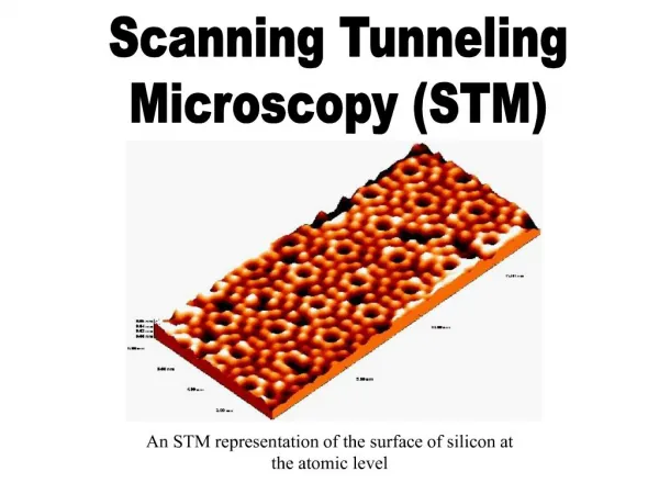
Scanning Tunneling Microscopy
Scanning Tunneling Microscopy. By Jingpeng Wang CHEM*7530 Feb 21. 2006. Invented by Binnig and Rohrer at IBM in 1981 (Nobel Prize in Physics in 1986). Introduction. Binnig also invented the Atomic Force Microscope(AFM) at Stanford University in 1986. Introduction.

Scanning Tunneling Microscopy
E N D
Presentation Transcript
Scanning Tunneling Microscopy By Jingpeng Wang CHEM*7530 Feb 21. 2006
Invented by Binnig and Rohrer at IBM in 1981 (Nobel Prize in Physics in 1986). Introduction • Binnig also invented the Atomic Force Microscope(AFM) at Stanford University in 1986.
Introduction • Topographic (real space) images • Spectroscopic (electronic structure, density of states) images
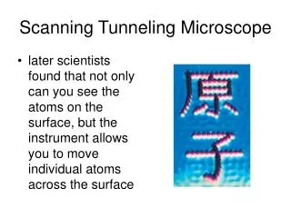
Atomic resolution, several orders of magnitude better than the best electron microscope Quantum mechanical tunnel-effect of electron In-situ: capable of localized, non-destructive measurements or modifications material science, physics, semiconductor science, metallurgy, electrochemistry, and molecular biology Scanning Probe Microscopes (SPM): designed based on the scanning technology of STM Introduction
Theory and Principle Tunneling Current • A sharp conductive tip is brought to within a few Angstroms of the surface of a conductor (sample). • The surface is applied a bias voltage, Fermi levels shift • The wave functions of the electrons in the tip overlap those of the sample surface • Electrons tunnel from one surface to the other of lower potential.
Theory and Principle • The tunneling system can be described as the model of quantum mechanical electron tunneling between two infinite, parallel, plane metal surfaces EF is the Fermi level ψ is the wave function of the electron Ф is the work function of the metal. Electrons tunnel through a rectangular barrier.
Theory and Principle • The tunneling current can be calculated from Schrödinger equation (under some further simplifications of the model). • It is the tunneling current; V is the sample bias • Фav is the average work function (barrier height), about 4 eV above the Fermi energy for a clean metal surface • d is the separation distance Tunneling current exhibits an exponentially decay with an increase of the separation distance! Exponential dependence leads to fantastic resolutions. Order of 10-12 m in the perpendicular direction and ~10-10 m in the parallel directions
Theory and Principle How tunneling works ? Simple answer • In classical physics e flows are not possible without a direct connection by a wire between two surfaces • On an atomic scale a quantum mechanical particle behaves in its wave function. • There is a finite probability that an electron will “jump” from one surface to the other of lower potential. "... I think I can safely say that nobody understands Quantum Mechanics"Richard P. Feynman
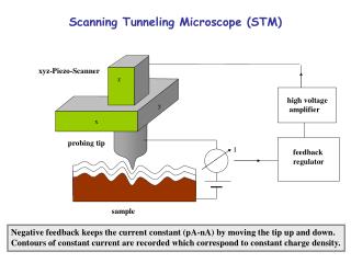
Experimental methods Basic Set-up • the sample you want to study • a sharp tip mounted on a piezoelectric crystal tube to be placed in very close proximity to the sample • a mechanism to control the location of the tip in the x-y plane parallel to the sample surface • a feedback loop to control the height of the tip above the sample (the z-axis)
How to operate? Raster the tip across the surface, and using the current as a feedback signal. The tip-surface separation is controlled to be constant by keeping the tunneling current at a constant value. The voltage necessary to keep the tip at a constant separation is used to produce a computer image of the surface.
What an STM measures?------local density of states Each plane represents a different value of the tip-sample bias V, and the lateral position on the plane gives the x,y position of the tip. Filled states are given in red. The plane at the Fermi energy (V=0) is shown in blue.
Experimental Optimization • Control of environment vibration: • building the instrument with sufficient mechanical rigidity; • hung on a double bungee cord sling to manage vibration; • vibration isolation systems have also been made with springs and frames; • operate at night with everything silent. • Ultrahigh vacuum (UHV): to avoid contamination of the samples from the surrounding medium. (The STM itself does not need vacuum to operate; it works in air as well as under liquids.) • Using an atomically sharp tip.
Instrumentation details Pure metals (W, Au) Alloys (Pt-Rh, Pt-Ir) Chemically modified conductor (W/S, Pt-Rh/S, W/C…) • STM tip: atomically sharp needle and terminates in a single atom Preparation of tips: cut by a wire cutter and used as is cut followed by electrochemical etching Electrochemical etching of tungsten tips. A tungsten wire, typically 0.25 mm in diameter, is vertically inserted in a solution of 2M NaOH. A counter electrode, usually a piece of platinum or stainless steel, is kept at a negative potential relative to the tungsten wire. The etching takes a few minutes. When the neck of the wire near the interface becomes thin enough, the weight of the wire in electrolyte fractures the neck. The lower half of the wire drops off.
Typical Applications of STM Electrochemical STM (ECSTM) • Powerful imaging tool, directly visualize electrochemical processes in-situ and in real space at molecular or atomic levels. • Such interfacial electrochemical studies have been dramatically expanded over the past decade, covering areas in electrode surfaces, metal deposition, charge transfer, potential-dependent surface morphology, corrosion, batteries, semiconductors, and nanofabrication. • Events in the EC data correlate with changes in the topography of the sample surface.
Electrochemical STM • Three-electrode system+ STM: the STM tip may also become working electrode as well as a tunneling tip. • Need to insulate all but the very end of the STM tip with Apiezon wax to minimize faradic currents, which can be several orders of magnitude larger than the tunneling current and make atomic resolution unfeasible or even trigger other unwanted electrochemical reactions.
Imaging the structure of electrode surface STM images of the Au (100) electrode surface (Left) Au (100) electrode in 0.1 M H2SO4 at -0.25 V vs. SCE, where potential-induced reconstruction proceeds. The initially unreconstructed surface is being gradually transformed into the reconstructed form. (Right) The zoom shows a section of the surface, 3/4 of which has already been reconstructed; one single reconstruction row on the left hand side is seen to grow from bottom to the top of the image. STM images of the Au(111) electrode surface (Right) the reconstructed surface at negative charge densities (Left) unreconstructed surface at positive charge densities
Metal deposition When applying an potential negative of the equilibrium potential Er to cathode, bulk deposition of metal takes place. As a nucleation-and-growth process, deposition of metal preferentially occurs at the surface defects, such as steps or screw dislocations. STM images of Au(111) surface in 5 mM H2SO4 + 0.05 mM CuSO4 before (panel a) and during (panel b) copper deposition. The bare gold surface has atomically flat terraces separated by three monoatomic high steps. After a potential step to negative values, deposition of bulk Cu occurs almost preferentially at the monoatomic high steps, namely, the growing Cu clusters are decorating the gold surface defects.
STM-based electrochemical nanotechnology STM tip: a tool for manipulating individual atoms or molecules on substrate surface and directing them continuously to predetermined positions ECSTM tip-generated entities are clearly larger than single atoms due to their low stability to survive electrochemical environment at room temperature. Tip crash method: (surface damaged ) use the tip to create surface defects, which then acted as nucleation centers for the metal deposition at pre-selected positions. Jump-to-contact method: (surface undamaged ) metal is first deposited onto the tip from electrolyte, then the metal-loaded tip approaches the surface to form a connective neck between tip and substrate. Upon retreat of the tip and applying a pulsed voltage, the neck breaks, leaving a metal cluster on the substrate. Continued metal deposition onto the tip supplies enough material for the next cluster generation.
Application of STM in SAMs • Electrochemistry can be used to manipulate the adsorbates themselves by electrolytically cleaving the Au–SR bond at the interface, resulting in a free thiolate and Au. • Electrochemical desorption: RS-Au + e- RS- + Au Different thiols have different reductive potentials, varying from -0.75 V to -1.12 V The I-V curves obtained from 4 kinds of tunneling structures (from left to right): bare Pt-Ir tip over thiols, C60 tip over thiols, bare Pt-Ir tip over C60, C60 tip over C60.
Concluding remarks STM is one the most powerful imaging tools with an unprecedented precision. Disadvantage of STM: Making atomically sharp tips remains something of a dark art! External and internal vibrations from fans, pumps, machinery, building movements, etc. are big problems. UHV-STM is not easy to built and handle. The STM can only scan conductive surfaces or thin nonconductive films and small objects deposited on conductive substrates. It does not work with nonconductive materials, such as glass, rock, etc. The spatial resolution of STM is fantastic, but the temporal resolution is typically on the order of seconds, which prevents STM from imaging fast kinetics of electrochemical process.
Reference [13] Tim McArdle,Stuart Tessmer, Summer 2002,Michigan State University,Operation of a Scanning Tunneling Microscope(available online) [14] J.C. Davis Group, LASSP, Cornell University; http://people.ccmr.cornell.edu/~jcdavis/stm/background/STMmeasurements.htm [15] Mixing electrochemistry with microscopy,James P. Smith; http://elchem.kaist.ac.kr/publication/paper/misc/2001_AC_39A/2001_AC_39A.htm [16] D.M. Kolb,Surface Science 500 (2002) 722–740 [17] Cavallini, M and Biscarini, F. Review of Scientific Instruments, 71 (12) December 2000. [18] L. A. Nagahara, T. Thundat, and S. M. Lindsay; Review of Scientific Instruments Vol 60(10) pp. 3128-3130. October 1989 [19]S.Wu.Tian;Application of Electrochemical Scanning Tunnelling Microscopy in Electrochemistry; http://www.nsfc.gov.cn/nsfc/cen/HTML/jw4/402/01/1-2.html [20] J.Lipkowski, 1999; Alcan lecture, Canadian J. Chem. , 77, 1168-1176. [21]T. Will, M. Dietterle, D.M. Kolb, The initial stages of electrolytic Cu deposition: an atomistic view, in: A.A. Gewirth, H. Siegenthaler (Eds.), Nanoscale Probes of the Solid/Liquid Interface, Nato ASI, vol. E288, Kluwer, Dordrecht, 1995, p. 137. [22]W. Li, J.A. Virtanen, R.M. Penner, Appl. Phys. Lett. 60 (1992) 1181. [23] W. Schindler, D. Hofmann, J. Kirschner, J. Appl. Phys. 87 (2000) 7007. [24] D.M. Kolb , G.E. Engelmann, J.C. Ziegler; Solid State Ionics 131 (2000) 69–78 [25] D.M. Kolb, G.E. Engelmann, J.C. Ziegler; Sol. State Ionics 131 (2000) 69. [26] N.J. Tao, C.Z. Li, H.X. He; Journal of Electroanalytical Chemistry 492 (2000) 81–93 • [1] (a)G. Binnig and H. Rohrer, U.S. Patent No. 4,343,993 (10 August 1982). (b)Binnig, G., Rohrer, H., et al., (1982) Phys. Rev. Lett., 49:57. • [2] G. Binnig, et al., Phys. Rev. Lett., 56, 930-933 (1986). • [3] Electrochemical Scanning Tunneling Microscope (ECSTM)http://www.soton.ac.uk/~surface/suec_stm.shtml • [4] The Tunneling Current - A Simple Theory http://wwwex.physik.uni-ulm.de/lehre/methmikr/buch/node5.html • [5] Scanning Tunneling Microscopy http://www.physnet.uni-hamburg.de/home/vms/pascal/stm.htm • [6] Scanning Tunneling Microscopy Basics http://nanowiz.tripod.com/stmbasic/stmbasic.htm • [7] Scanning Tunneling Microscopy http://www.chembio.uoguelph.ca/thomas/stm_research.html • [8] Interpretation of Scanning Tunneling Microscopy and Spectroscopy of Magnetic Metal Surfaces by Electron Theory, Daniel Wortmann,,Universityat Dortmund, Februar 2000,available online. • [9]The Scanning Tunneling Microscope-What it is and how it works http://www.iap.tuwien.ac.at/www/surface/STM_Gallery/stm_schematic.html • [10] A short history of Scanning Probe Microscopy http://hrst.mit.edu/hrs/materials/public/STM_thumbnail_history.htm • [11] Davis Baird,Ashley Shew,Department of Philosophy, University of South Carolina, Columbia, Probing the History of Scanning Tunneling Microscopy, October 2002,available online. • [12] Lecture 4,Scanning Tunneling Microscopy, CHM8490/8190, Spring 2000, Dr. Gang-yu Liu(available online)