Download
1 / 88
890 likes | 1.09k Vues
Sequential Circuits Chapter 6 Henry Hexmoor-- SIUC. A Sequential circuit contains: Storage elements: Latches or Flip-Flops Combinatorial Logic: Implements a multiple-output switching function

E N D
Sequential CircuitsChapter 6 Henry Hexmoor-- SIUC Henry Hexmoor
A Sequential circuit contains: Storage elements:Latches or Flip-Flops Combinatorial Logic: Implements a multiple-output switching function Inputs are signals from the outside. Outputs are signals to the outside. Other inputs, State or Present State, are signals from storage elements. The remaining outputs, Next State are inputs to storage elements. Outputs Inputs Combina-tional Logic Storage Elements Next State State Introduction to Sequential Circuits Henry Hexmoor
Combinatorial Logic Next state functionNext State = f(Inputs, State) Mealy circuit:Outputs = g(Inputs, State) Moore circuit:Outputs = h(State) Output function type depends on specification and affects the design significantly Outputs Inputs Combina-tional Logic Storage Elements Next State State Sequential Circuits Henry Hexmoor
Depends on the times at which: storage elements observe their inputs, and storage elements change their state Synchronous Behavior defined from knowledge of its signals at discrete instances of time Storage elements observe inputs and can change state only in relation to a timing signal (clock pulses from a clock) Asynchronous Behavior defined from knowledge of inputs an any instant of time and the order in continuous time in which inputs change If clock just regarded as another input, all circuits are asynchronous! Nevertheless, the synchronous abstraction makes complex designs tractable! Types of Sequential Circuits Henry Hexmoor
In order to understand the time behavior of a sequential circuit we use discrete event simulation. Rules: Gates modeled by anideal(instantaneous) function and a fixed gate delay Any change in input values is evaluated to see if it causes a change in output value Changes in output values are scheduled for the fixed gate delay after the input change At the time for a scheduled output change, the output value is changed along with any inputs it drives Discrete Event Simulation Henry Hexmoor
Suppose gates with delay n ns are represented for n = 0.2 ns, n = 0.4 ns,n = 0.5 ns, respectively: 0.2 0.5 0.4 Gate Delay Models Henry Hexmoor
Consider a simple 2-input multiplexer: With function: Y = A for S = 0 Y = B for S = 1 Glitch” is due to delay of inverter A Y S B 0.2 0.5 0.4 0.4 S Circuit Delay Model A B S Y Henry Hexmoor
A memory should have at least three properties. 1. It should be able to hold a value. 2. You should be able to read the value that was saved. 3. You should be able to change the value that’s saved. We’ll start with the simplest case, a one-bit memory. 1. It should be able to hold a single bit, 0 or 1. 2. You should be able to read the bit that was saved. 3. You should be able to change the value. Since there’s only a single bit, there are only two choices: Set the bit to 1 Reset, or clear, the bit to 0. What is memory Henry Hexmoor
How can a circuit “remember” anything, when it’s just a bunch of gates that produce outputs according to the inputs? The basic idea is to make a loop, so the circuit outputs are also inputs. Here is one initial attempt, shown with two equivalent layouts: Does this satisfy the properties of memory? These circuits “remember” Q, because its value never changes. (Similarly, Q’ never changes either.) We can also “read” Q, by attaching a probe or another circuit. But we can’t change Q! There are no external inputs here, so we can’t control whether Q=1 or Q=0. Basic storage Henry Hexmoor
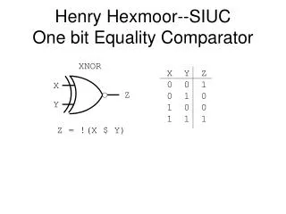
A really confusing circuit • Let’s use NOR gates instead of inverters. The SR latch (right) has two inputs S and R, which will let us control the outputs Q and Q’. • Here Q and Q’ feed back into the circuit. They’re not only outputs, they’re also inputs! • To figure out how Q and Q’ change, we have to look at not only the inputs S and R, but also the current values of Q and Q’: Qnext = (R + Q’current)’ Q’next = (S + Qcurrent)’ • Let’s see how different input values for S and R affect this thing. Henry Hexmoor
Timing diagrams are useful in understanding how sequential circuits work. Here is a diagram which shows an example of how our latch outputs change with inputs RS=01. 0. Suppose that initially, Q = 0 and Q’= 1. 1. Since S=1, Q’ will change from 1 to 0 after one NOR-gate delay (marked by vertical lines in the diagram for clarity). 2. This change in Q’, along with R=0, causes Q to become 1 after another gate delay. 3. The latch then stabilizes until S or R change again. Latch delays Qnext = (R + Q’current)’ Q’next = (S + Qcurrent)’ 0 1 2 3 4 S R Q Q’ Henry Hexmoor
This little table shows that our latch provides everything we need in a memory: we can set it, reset it, and remember the current value. The output Q represents the data stored in the latch. It is sometimes called the state of the latch. We can expand the table above into a state table, which explicitly shows that the next values of Q and Q’ depend on their current values, as well as on the inputs S and R. SR latches are memories! Henry Hexmoor
There are several varieties of latches. You can use NAND instead of NOR gates to get a S’R’ latch. This is just like an SR latch, but with inverted inputs, as you can see from the table. You can derive this table by writing equations for the outputs in terms of the inputs and the current state, just as we did for the SR latch. S’R’ latch Henry Hexmoor
Here is an SR latch with a control input C. Notice the hierarchical design! The dotted blue box is the S’R’ latch from the previous slide. The additional NAND gates are simply used to generate the correct inputs for the S’R’ latch. The control input acts just like an enable. An SR latch with a control input Henry Hexmoor
Finally, a D latch is based on an S’R’ latch. The additional gates generate the S’ and R’ signals, based on inputs D (“data”) and C (“control”). When C = 0, S’ and R’ are both 1, so the state Q does not change. When C = 1, the latch output Q will equal the input D. No more messing with one input for set and another input for reset! Also, this latch has no “bad” input combinations to avoid. Any of the four possible assignments to C and D are valid. D Q C Q D Q Q C D latch Henry Hexmoor
To describe combinational circuits, we used Boolean expressions and truth tables. With sequential circuits, we can still use expression and tables, but we can also use another form called a state diagram. We draw one node for each state that the circuit can be in. Latches have only two states: Q=0 and Q=1. Arrows between nodes are labeled with “input/output” and indicate how the circuit changes states and what its outputs are. In this case the state and the output are the same. Basically the same as the finite state automata. Here’s a state diagram for a D latch with inputs D and C. 0x/1 0x/0 11/1 Q=0 Q=1 10/0 Sequential circuits and state diagrams Henry Hexmoor
We can connect some latches, acting as memory, to an ALU. Let’s say these latches contain some value that we want to increment. The ALU should read the current latch value. It applies the “G = X + 1” operation. The incremented value is stored back into the latches. At this point, we have to stop the cycle, so the latch value doesn’t get incremented again by accident. One convenient way to break the loop is to disable the latches. D Q Latches C +1 S ALU G X Using latches in real life Henry Hexmoor
The problem is exactly when to disable the latches. You have to wait long enough for the ALU to produce its output, but no longer. But different ALU operations have different delays. For instance, arithmetic operations might go through an adder, whereas logical operations don’t. Changing the ALU implementation, such as using a carry-lookahead adder instead of a ripple-carry adder, also affects the delay. In general, it’s very difficult to know how long operations take, and how long latches should be enabled for. D Q Latches C +1 S ALU G X The problem with latches Henry Hexmoor
A sequential circuit has memory. It may respond differently to the same inputs, depending on its current state. Memories can be created by making circuits with feedback. Latches are the simplest memory units, storing individual bits. It’s difficult to control the timing of latches in a larger circuit. Next, we’ll improve upon latches with flip-flops, which change state only at well-defined times. We will then use flip-flops to build all sequential circuits. Memory Summary Henry Hexmoor
Latches introduce new problems: We need to know when to enable a latch. We also need to quickly disable a latch. In other words, it’s difficult to control the timing of latches in a large circuit. We solve these problems with two new elements: clocks and flip-flops Clocks tell us when to write to our memory. Flip-flops allow us to quickly write the memory at clearly defined times. Used together, we can create circuits without worrying about the memory timing. Flip-Flops Henry Hexmoor
Our example used latches as memory for an ALU. Let’s say there are four latches initially storing 0000. We want to use an ALU to increment that value to 0001. Normally the latches should be disabled, to prevent unwanted data from being accidentally stored. In our example, the ALU can read the current latch contents, 0000, and compute their increment, 0001. But the new value cannot be stored back while the latch is disabled. D +1 Q Latches C 0001 0000 0 S ALU G X Making latches work right Henry Hexmoor
After the ALU has finished its increment operation, the latch can be enabled, and the updated value is stored. The latch must be quickly disabled again, before the ALU has a chance to read the new value 0001 and produce a new result 0010. 0001 D D 0001 +1 +1 Q Q Latches Latches C C 0010 0001 1 0 S S ALU ALU G G X X Writing to the latches Henry Hexmoor
So to use latches correctly within a circuit, we have to: Keep the latches disabled until new values are ready to be stored. Enable the latches just long enough for the update to occur. There are two main issues we need to address: How do we know exactly when the new values are ready? We’ll add another signal to our circuit. When this new signal becomes 1, the latches will know that the ALU computation has completed and data is ready to be stored. How can we enable and then quickly disable the latches? This can be done by combining latches together in a special way, to form what are called flip-flops. Two main issues Henry Hexmoor
A clock is a special device that whose output continuously alternates between 0 and 1. The time it takes the clock to change from 1 to 0 and back to 1 is called the clock period, or clock cycle time. The clock frequency is the inverse of the clock period. The unit of measurement for frequency is the hertz. Clocks are often used to synchronize circuits. They generate a repeating, predictable pattern of 0s and 1s that can trigger certain events in a circuit, such as writing to a latch. If several circuits share a common clock signal, they can coordinate their actions with respect to one another. This is similar to how humans use real clocks for synchronization. clock period Clocks and synchronization Henry Hexmoor
Clocks are used extensively in computer architecture. All processors run with an internal clock. Modern chips run at frequencies above 3.2 GHz. This works out to a cycle time smaller than 0.31 ns! Memory modules are often rated by their clock speeds too—examples include “PC133” and “DDR400” memory. Be careful...higher frequencies do not always mean faster machines! You also have to consider how much work is actually being done during each clock cycle. How much stuff can really get done in just 0.31 ns. More about clocks Henry Hexmoor
We can use a clock to synchronize our latches with the ALU. The clock signal is connected to the latch control input C. The clock controls the latches. When it becomes 1, the latches will be enabled for writing. The clock period must be set appropriately for the ALU. It should not be too short. Otherwise, the latches will start writing before the ALU operation has finished. It should not be too long either. Otherwise, the ALU might produce a new result that will accidentally get stored, as we saw before. The faster the ALU runs, the shorter the clock period can be. D +1 Q Latches C S ALU G X Synchronizing our example Henry Hexmoor
The second issue was how to enable a latch for just an instant. Here is the internal structure of a D flip-flop. The flip-flop inputs are C and D, and the outputs are Q and Q’. The D latch on the left is the master, while the SR latch on the right is called the slave. Note the layout here. The flip-flop input D is connected directly to the master latch. The master latch output goes to the slave. The flip-flop outputs come directly from the slave latch. Flip-flops Henry Hexmoor
The D flip-flop’s control input C enables either the D latch or the SR latch, but not both. When C = 0: The master latch is enabled, and it monitors the flip-flop input D. Whenever D changes, the master’s output changes too. The slave is disabled, so the D latch output has no effect on it. Thus, the slave just maintains the flip-flop’s current state. D flip-flops when C=0 Henry Hexmoor
As soon asC becomes 1, The master is disabled. Its output will be the last D input value seen just before C became 1. Any subsequent changes to the D input while C = 1 have no effect on the master latch, which is now disabled. The slave latch is enabled. Its state changes to reflect the master’s output, which again is the D input value from right when C became 1. D flip-flops when C=1 Henry Hexmoor
This is called a positive edge-triggered flip-flop. The flip-flop output Q changes only after the positive edge of C. The change is based on the flip-flop input values that were present right at the positive edge of the clock signal. The D flip-flop’s behavior is similar to that of a D latch except for the positive edge-triggered nature, which is not explicit in this table. Positive edge triggering Henry Hexmoor
One last thing to worry about… what is the starting value of Q? We could set the initial value synchronously, at the next positive clock edge, but this actually makes circuit design more difficult. Instead, most flip-flops provide direct, or asynchronous, inputs that let you immediately set or clear the state. You would “reset” the circuit once, to initialize the flip-flops. The circuit would then begin its regular, synchronous operation. Here is a LogicWorks D flip-flop with active-low direct inputs. Direct inputs Direct inputs to set or reset the flip-flop S’R’ = 11 for “normal” operation of the D flip-flop Henry Hexmoor
At power up or at reset, all or partof a sequential circuit usually isinitialized to a known state beforeit begins operation This initialization is often doneoutside of the clocked behaviorof the circuit, i.e., asynchronously. Direct R and/or S inputs that control the state of the latches within the flip-flops are used for this initialization. For the example flip-flop shown 0 applied to R resets the flip-flop to the 0 state 0 applied to S sets the flip-flop to the 1 state S D Q C Q R Direct Inputspage 256 Henry Hexmoor
We can use the flip-flops’ direct inputs to initialize them to 0000. During the clock cycle, the ALU outputs 0001, but this does not affect the flip-flops yet. C Q0 G0 0001 0000 0000 D D +1 +1 Q Q Flip-flops Flip-flops C C C Q0 G0 S S ALU ALU G G X X Our example with flip-flops Henry Hexmoor
The ALU output is copied into the flip-flops at the next positive edge of the clock signal. The flip-flops automatically “shut off,” and no new data can be written until the next positive clock edge... even though the ALU produces a new output. C Q0 G0 0010 0001 0001 0001 D D +1 +1 Q Q Flip-flops Flip-flops C C C Q0 G0 S S ALU ALU G G X X Example continued Henry Hexmoor
We can make different versions of flip-flops based on the D flip-flop, just like we made different latches based on the S’R’ latch. A JK flip-flop has inputs that act like S and R, but the inputs JK=11 are used to complement the flip-flop’s current state. A T flip-flop can only maintain or complement its current state. Flip-flop variations Henry Hexmoor
The tables that we’ve made so far are called characteristic tables. They show the next state Q(t+1) in terms of the current state Q(t) and the inputs. For simplicity, the control input C is not usually listed. Again, these tables don’t indicate the positive edge-triggered behavior of the flip-flops that we’ll be using. Characteristic tables Henry Hexmoor
We can also write characteristic equations, where the next state Q(t+1) is defined in terms of the current state Q(t) and inputs. Characteristic equations Q(t+1) = D Q(t+1) = K’Q(t) + JQ’(t) Q(t+1) = T’Q(t) + TQ’(t) = T Q(t) Henry Hexmoor
To use memory in a larger circuit, we need to: Keep the latches disabled until new values are ready to be stored. Enable the latches just long enough for the update to occur. A clock signal is used to synchronize circuits. The cycle time reflects how long combinational operations take. Flip-flops further restrict the memory writing interval, to just the positive edge of the clock signal. This ensures that memory is updated only once per clock cycle. There are several different kinds of flip-flops, but they all serve the same basic purpose of storing bits. Flip Flop Summary Henry Hexmoor
Master-Slave:Postponed outputindicators Edge-Triggered:Dynamicindicator S S D D R R C C D with 0 Control SR D with 1 Control SR (a) Latches S S D D C C R R C C Triggered D Triggered D Triggered SR Triggered SR (b) Master-Slave Flip-Flops D D C C Triggered D Triggered D (c) Edge-Triggered Flip-Flops Standard Symbols for Storage Elements Henry Hexmoor
ts - setup time th - hold time tw - clockpulse width tpx - propa-gation delay tPHL - High-to-Low tPLH - Low-to-High tpd - max (tPHL, tPLH) Flip-Flop Timing Parameters- page 257 t t $ wH wH,min t t $ C wL wL,min t t s h / R S t p-,min t p-,max Q (a) Pulse-triggered (positive pulse) t t $ wH,min wH t t $ C wL wL,min t t s h D t p-,min t p-,max Q (b) Edge-triggered (negative edge) Henry Hexmoor
General Model Current Stateat time (t) is stored in an array offlip-flops. Next State at time (t+1) is a Boolean function of State and Inputs. Outputs at time (t) are a Boolean function of State (t) and (sometimes) Inputs (t). Inputs Combina-tional Logic Outputs Storage Elements Next State State CLK Sequential Circuit Analysis6-4 Henry Hexmoor
Input: x(t) Output:y(t) State: (A(t), B(t)) What is the Output Function? What is the Next State Function? x A Q D A Q C B Q D CP Q C y Example 1 (Figure 6-17) Henry Hexmoor
Boolean equations for the functions: A(t+1) = A(t)x(t) + B(t)x(t) B(t+1) = A(t)x(t) y(t) = x(t)(B(t) + A(t)) Example 1 (from Figure 6-17) (page 260) x A Q D A Q C Next State B Q D CP Q' C y Output Henry Hexmoor
State table – a multiple variable table with the following four sections: Present State – the values of the state variables for each allowed state. Input – the input combinations allowed. Next-state – the value of the state at time (t+1) based on the present state and the input. Output – the value of the output as a function of the present state and (sometimes) the input. From the viewpoint of a truth table: the inputs are Input, Present State and the outputs are Output, Next State State Table Characteristics Henry Hexmoor
The state table can be filled in using the next state and output equations: A(t+1) = A(t)x(t) + B(t)x(t) B(t+1) =A (t)x(t) y(t) =x (t)(B(t) + A(t)) Present State Input Next State Output A(t) B(t) x(t) A(t+1) B(t+1) y(t) 0 0 0 0 0 0 0 0 1 0 1 0 0 1 0 0 0 1 0 1 1 1 1 0 1 0 0 0 0 1 1 0 1 1 0 0 1 1 0 0 0 1 1 1 1 1 0 0 Example 1: State Table (from Figure 6-17) Henry Hexmoor
2-dimensional table that matches well to a K-map. Present state rows and input columns in Gray code order. A(t+1) = A(t)x(t) + B(t)x(t) B(t+1) =A (t)x(t) y(t) =x (t)(B(t) + A(t)) Present Next State Output State x(t)=0 x(t)=1 x(t)=0 x(t)=1 A(t) B(t) A(t+1)B(t+1) A(t+1)B(t+1) y(t) y(t) 0 0 0 0 0 1 0 0 0 1 0 0 1 1 1 0 1 0 0 0 1 0 1 0 1 1 0 0 1 0 1 0 Example 1: Alternate State Table Henry Hexmoor
The sequential circuit function can be represented in graphical form as a state diagram with the following components: A circle with the state name in it for each state A directed arc from the Present State to the Next State for each state transition A label on each directed arc with the Input values which causes the state transition, and A label: On each circle with the output value produced, or On each directed arc with the output value produced. State Diagrams Henry Hexmoor
Label form: On circle with output included: state/output Moore type output depends only on state On directed arc with the output included: input/output Mealy type output depends on state and input State Diagrams Henry Hexmoor
Which type? Diagram getsconfusing forlarge circuits For small circuits,usually easier tounderstand thanthe state table x=0/y=0 x=0/y=1 x=1/y=0 A B 1 0 0 0 x=0/y=1 x=1/y=0 x=1/y=0 x=0/y=1 1 1 0 1 x=1/y=0 Example 1: State Diagram Henry Hexmoor
Sequential Circuits or Sequential Machines are also called Finite State Machines (FSMs). Two formal models exist: In contemporary design, models are sometimes mixed Moore and Mealy Moore and Mealy Models • Moore Model • Named after E.F. Moore. • Outputs are a function ONLY of states • Usually specified on the states. • Mealy Model • Named after G. Mealy • Outputs are a function of inputs AND states • Usually specified on the state transition arcs. Henry Hexmoor