Binary Parallel Adders
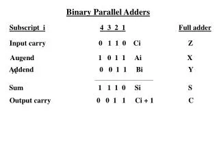
Binary Parallel Adders. Subscript i. 4 3 2 1. Full adder. Input carry 0 1 1 0 Ci Z. Augend 1 0 1 1 Ai X.


Binary Parallel Adders
E N D
Presentation Transcript
Binary Parallel Adders Subscript i 4 3 2 1 Full adder Input carry 0 1 1 0 Ci Z Augend 1 0 1 1 Ai X Addend 0 0 1 1 Bi Y A Sum 1 1 1 0 Si S Output carry 0 0 1 1 Ci + 1 C
B4 A4 A3 B3 A1 B2 B1 A2 C1 C5 C4 C2 C3 FA FA FA FA 0 S4 S3 S1 S2 4-BIT FULL ADDER • An n-bit parallel adder requires n full adders • An IC of 4-bit FA has 14 terminals • It is an MSI function • The classical method would require a truth table with 512 entries • (9 input variable) (too cumbersome)
Not used C5 S1 S2 S3 S4 A1 A2 A3 A4 Excess-3 BCD INPUT Output 1 B1 B2 B3 B4 0 C1 BCD -to -Excess 3 Code Converter
D’ Z CD D C Y (C+D)’ C+D B X W A
Classical Method • Truth table for four inputs • K-maps for four outputs • Algebraic manipulation of expressions • Logic diagram using gates 4 x AND gates, 4 x OR gates & 3 x inverters • Requires 3 IC packages & 14 wire connections (excluding 1/0 connections) Alternate Design Methods 1 IC package , MS1 function , 5 wire connections (excluding 1/O connections)
Derivation of a BCD adder Input Binary Sum Output B C D Sum
Addend Augend 4-bit binary adder carry out carry in K Z8 Z4 Z2 Z1 Output Carry 0 1 0 0 1 4-bit binary adder BLOCK DIAGRAM OF A BCD ADDER S2 S8 S4 S1
x’ y’ z’ D0 x’ y’ z D1 z x’ y z’ D2 y x’ y z D3 x y’ z’ D4 x Input lines = n Output lines = 2n (Maximum) n – to – m decoder M ≤ 2n x y’ z D5 x y z’ D6 x y z D7 A 3 – to – 8 line decoder (Binary – to – Octal application)
Truth table of a 3 – to – 8 line decoder Outputs Inputs
Design a BCD – to – Decimal Decoder y D0 = w’ x’ y’ z’ D1 = w’ x’ y’ z D2 = x’ y z’ D3 = x’ y z D4 = x y’ z’ D5 = x y’ z D6 = x y z’ D7 = x y z D8 = w z’ D9 = w z yz 00 01 11 10 wx 00 D0 D1 D3 D2 01 D4 D5 D7 D6 x 11 X X X X w 10 D8 D9 X X z Map for simplifying a BCD – to – decimal decoder
D0 = w’ x’ y’ z’ D1 = w’ x’ y’ z w D2 = x’ y z’ D3 = x’ y z x D4 = x y’ z’ D5 = x y’ z D6 = x y z’ y D7 = x y z D8 = w z’ z D9 = w z BCD – TO – DECIMAL DECODER ( 4 – LINE TO 10 – LINE)
PARTIAL TRUTH TABLE Inputs Outputs
S (x, y, z) = (1, 2, 4, 7) c (x, y, z) = (3, 5, 6, 7) s x 22 3 x 8 y 21 decoder c z 20 Implementation of a full adder with a decoder and two OR gates
DEMULTIPLEXERS • A decoder with an enable input can function as a demultiplexer. It receives information on a single line and transmits this information on one of 2n possible output lines. • A 2 – to – 4 line decoder with E input is shown • When E = 0, the circuit operates as a decoder with comlemented outputs.
The decoder can function as a demultiplexer if E line is taken as a data input line and A & B lines are taken as the selection line. • 2 decoders (3x8) can be connected to form a larger decoder circuit (4x16) when: W = 0, top decoder is inabled (0000 – 0111) W = 1, bottom decoder is enabled (1000 – 1111) • Digital function can be easily expanded to accommodate more inputs and outputs by using e lines
B Demultiplexer (A’ B’ )’ = A + B A0011 B0101 D0 (A’ B )’ = A + B’ D1 (A B’ )’ = A’ + B D2 A (A B )’ = A’ + B’ D3 E (a) LOGIC DIAGRAM WITH NAND GATES
TRUTH TABLE A 2 – TO – 4 LINE DECODER WITH ENABLE E INPUT
2 X 4 Decoder D0 D0 A D1 D1 1 X 4 Inputs Demultiplexer D2 D2 B D3 D3 Input E E Enable B A Select • Decoder with enable can • function as demultiplexer (b) Demultiplexer
X 3 X 8 D0 to D7 y Decoder 0000 to 0111 z E W 3 X 8 D8 to D15 Decoder 1000 to 1111 E A 4x16 Decoder Constructed with two 3x8 Decoders
ENCODERS • An encoder produces a reverse operation of a decoder Input lines ≤ 2n Output lines = n • An octal-to-binary encoder circuit has 8 inputs and 3 outputs. • Only one input line can be equal to one at any time. Possible input combinations = 28 = 256 Meaningful combinations = 8 Don’t care conditions = 248
Priority encoder establishes an input priority to ensure that the highest priority input line is encoded. D2 If input 1 D5 Output line D5 is encoded because of higher–priority • When D0 is not connected to any OR gate, then binary output is 000.
D0 x = D4+ D5 + D6 + D7 D1 D2 D3 y = D2+ D3 + D6 + D7 D4 D5 D6 z = D1+ D3 + D5 + D7 D7 Octal to binary encoder
TRUTH TABLE INPUTS (Octal) D0 D1 D2 D3 D4 D5 D6 D7 OUTPUTS (binary) x y z 0 0 0 0 0 1 0 1 0 0 1 1 1 0 0 1 0 1 1 1 0 1 1 1 0 1 0 0 0 0 0 0 0 1 0 1 0 0 0 0 0 0 2 0 0 1 0 0 0 0 0 3 0 0 0 1 0 0 0 0 4 0 0 0 0 1 0 0 0 5 0 0 0 0 0 1 0 0 6 0 0 0 0 0 0 1 0 7 0 0 0 0 0 0 0 1
Multiplexers • A digital multiplexer is a combinational circuit that selects binary information from one of many input lines and directs it to a single output line. input lines = 2n output lines = 1 selection lines = n • An example of 4-line-to-1-line shows that: input lines = 22 = 4 (I0, I1, I2 & I3) output lines = 1 (Y) selection lines = 2 (s0 & s1)
A multiplexer is also called a data selector since it selects one of many inputs and steers the binary information to the output line. • Multiplexer ICs can have an enable input to control the operation of the unit. When E is in disable state, outputs = 0. When E is in enable state, the circuit functions as a normal MUX. • The E strobe can used to expand two or more ICs (MUXs) to provide a larger number of inputs.
I0 inputs 0 1 2 3 4 x 1 MUX output I1 Y Y S0 S1 I2 S1 S0 Y 0 0 I0 0 1 I1 1 0 I2 1 1 I3 Select I3 S1 S0 (a) Logic Diagram A 4-to-1 Line Multiplexer (c) Function Table (b) Block Diagram
A1 Y1 A2 Y2 A3 Y3 A4 Y4 B1 Function Table E S Output Y 1 X all 0’s 0 0 Select A 0 1 Select B B2 B3 B4 S (Select) Quadruple 2-to-1 Line multiplexer E (Enable)
4 x MUXs • E = 1, Y1 -Y4 = 0 • When E = 0, S = 0: • Y1 = A1 • Y2 = A2 • Y3 = A3 • Y4 = A4 • When E = 0, S=1 Y1 = B1 ,Y2=B2, Y3=B3 & Y4=B4 Function Table E S Output Y 1 X all Os 0 0 Select A 0 1 Select B • Applications:- • Used for connecting 2 or more sources to a single • destination among computer units. • Used for constructing a common bus system
Boolean Function Implementation S1 S0 Example :- F(A,B,C)=Σ (1,3,5,6) Minterm A B C F 0 I0 0 0 0 0 1 1 1 1 0 0 1 1 0 0 1 1 0 1 0 1 0 1 0 1 0 1 2 3 4 5 6 7 0 1 0 1 0 1 1 0 I1 1 4 x 1 MUX F Y A I2 A’ I3 S1 S0 B C (a) Truth Table (c) Multiplexer Implementation I0 I1 I2 I3 It is possible to generate any function of n+1 variables with 2n-to-1 Multiplexer A’ 0 1 3 2 4 5 6 7 A 0 1 A A’ (b)Implementation Table Implementing F(A,B,C)= Σ (1,3,5,6) with a multiplexer
Alternate implementation for F(A,B,C)= Σ (1,3,5,6) I0 S1 I1 S0 4 x 1 MUX Y I2 A B C F I3 S1 s0 0 2 4 6 1 3 5 7 0 0 1 1 0 0 1 1 0 1 0 1 0 1 0 1 0 0 0 0 1 1 1 1 0 0 0 0 1 1 1 1 A B I0 I1 I2 I3 C F 0 2 6 C’ 4 1 3 5 7 C C C C C’ (b) Implementation Table (c) Multiplexer Implementation (a) Truth Table
A B C D F 0 0 0 0 0 0 0 0 1 1 1 1 1 1 1 1 0 0 0 0 1 1 1 1 0 0 0 0 1 1 1 1 0 0 1 1 0 0 1 1 0 0 1 1 0 0 1 1 0 1 0 1 0 1 0 1 0 1 0 1 0 1 0 1 1 1 0 1 1 0 0 0 1 1 0 0 0 0 0 1 0 1 2 3 4 5 6 7 8 9 10 11 12 13 14 15 Example:- F(A,B,C,D)= Σ (0,1,3,4,8,9,15) S2 S1 S0 1 I0 I1 0 I2 8 x 1 MUX I3 Y F I4 I5 I6 S1 S0 S2 I7 A B C D I0 I1 I2 I3 I4 I5 I6 I7 A’ 0 1 2 3 4 5 6 7 A 8 9 10 11 12 13 14 15 1 1 0 A’ A’ 0 0 A
READ ONLY MEMORY ROM • ROM is a device that includes both the decoder and the OR gates within a single IC package. • It is usually used to implement a complex comb. circuit in one IC package and eliminates all interconnecting wires between a decoder and OR gates. • It is a memory device in which binary information is stored fusing or breaking internal links in order to form required circuit paths. • If a ROM has: • input lines = n • output lines = m • Then: • Distinct Addresses (words) = 2n • Total no. of bits stored in ROM = 2n x m • (Where m denotes no. of bits per word)
32 x 8 ROM means: • Words = 32 of 8 bits each • Output lines = 8 • Input lines = 5 • Total bits = 256 (25 x 8) • Internal construction of a 32 x 4 ROM can be shown using a decoder and four OR gates ROM BLOCK DIAGRAM n inputs 2n xm ROM m outputs
Logic Construction of a 32 x 4 ROM (32words of 4 bits each) Total bits stored = 32 x 4 = 128 ADDRESS INPUTS MINTERMS A0 A1 5 x 32 decoder A2 A3 A4 INPUTS = 5 WORDS = 32 BITS/WORD = 4 OUTPUTS = 4 128 LINKS F1 F2 F3 F4
Combinational Logic Implementation - ROM For an n-input, m-output combinational circuit of a 2n x m ROM is needed The opening of the links is referred to as programming ROM program table gives the information for the required paths in the ROM Example: F1(A1, A0) = (1,2,3) F2(A1, A0) = (0,2) Truth Table A1 A0 F1 F2 0 0 0 1 0 1 1 0 1 0 1 1 1 1 1 0 Combinational circuit implementation with a 4 x 2 ROM is shown: With AND –OR gates With AND-OR-Inverter gates
00 A0 ROM with AND-OR gates 2 x 4 decoder 01 10 11 A1 TRUTH TABLE F1 F2 Combinational Circuit Implementation With a 4 x 2 ROM
Combinational Circuit Implementation With a 4 x 2 ROM 00 A0 ROM with AND-OR-INVERTER gates 2 x 4 decoder 01 10 11 A1 TRUTH TABLE F1 F2 F1 F2
Types of ROM Mask programming (ROM) PROM EPROM EAROM Uses to implement complex CC from truth tables to convert one binary code to another to implement arithmetic functions to display of characters on CRT to design microprogrammed control units
(i) TRUTH TABLE Example: Design a comb. circuit using a ROM. The circuit accepts a 3-bit number and generates an output binary number equal to the square of the input number.
(ii) (iii) A2 A0 A1 8 x 4 ROM F1 F2 F3 F4 0 B5 B0 B4 B3 B2 B1 BLOCK DIAGRAM ROM TRUTH TABLE ROM Implementation
Programmable Logic Array (PLA) • All the bit patterns available in the ROM are not used due to don’t care conditions which results into wastage of equipment • Size of the ROM required to convert a 12-bit card code to a 6-bit internal alphanumeric code: 4096 x 6 212 input output A-Z = 26 valid entries = 47 Numbers = 10 don’t care conditions = 4049 other char= 11 47 • It is more economical to use PLA (LSI) in such cases to avoid wastage.
Programmable Logic Array (PLA) • A block diagram of the PLA consists of: • n inputs • m outputs • k product terms • m sum terms • Output function: AND-OR form AND-OR-INVERTOR form • A typical PLA has : n = 16, m = 8, k = 48 programmed links PLAROM 2n * k + k * m + m 2n * m = 216 x 8 1928 524288 1 272
n x k Links m Links m Sum terms (OR gates) k x m Links K Product terms n x k Links Inputs m output (AND gates) PLA BLOCK DIAGRAM
IMPLEMENTATION OF PLA COMB CIRCUIT • Mask programmable (PLA) • Field programmable (FPLA) • PLA program table is required to program a PLA • Truth table of the comb. Circuit can be used to simplify the function to get the minimum AND gates (sum of products) • Paths are specified in its AND – OR or AND – OR - INVERT pattern by programming PLA • PLA program table contains: 1st column - lists product terms numerically 2nd column - specifies the required paths between OR gates and AND gates • T is written if the output inverter is to be bypassed • C is written if the output inverter is not to be bypassed • Variable is unprimed • 0 variable is primed • - Variable is absent
EXAMPLE#1 • F1 (A, B,C) = (4,5,7) • F2 (A,B,C) = (3,5,7)
B B BC BC 01 11 10 00 11 10 00 01 1 A’ A’ 0 0 0 0 0 0 0 0 0 1 1 1 1 1 0 0 A A 0 1 1 C C F2(A,B,C)=∑(3,5,7) F1(A,B,C)=∑(4,5,7) F2=AC+BC F1’F2’ = A’ + BC’ + C’ + A’B’ F’1F2 = A’ + BC’ + AC + BC F1F’2 = AB’ + AC + C’ + A’B’ F1F2 = AB’ + AC + BC So, the value k = 3. F1=AB’+AC F’2=C’ + A’B’ F’1=A’+BC’ Map simplification
TRUTH TABLE A B C F1 F2 0 0 0 0 0 0 0 1 0 0 0 1 0 0 0 0 1 1 0 1 1 0 0 1 0 1 0 1 1 1 1 1 0 0 0 1 1 1 1 1 Product term Inputs A B C Outputs F1 F2 1 2 3 1 0 - 1 - 1 - 1 1 1 - 1 1 - 1 AB’ AC BC T/C T T PLA Program table F1=AB’+AC F2=AC+BC STEPS REQUIRED IN PLA IMPLEMENTATION
A AB’ + AC AB’ 1 F1 B 2 AC + BC AC F2 BC n = 3 m = 2 K = 3 K * m (6) 3 C + m (2) PLA Links = 26 PLA with 3 inputs, 3 product terms, and 2 outputs; it implements the combinational circuit
EXAMPLE#2 F1(A,B,C)=∑(3,5,6,7) F2(A,B,C)=∑(0,2,4,7)