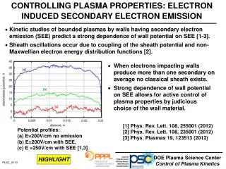
Secondary electron detector
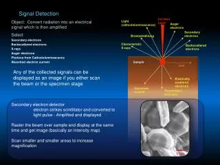
Signal Detection. Incident beam. Object: Convert radiation into an electrical signal which is then amplified Select Secondary electrons Backscattered electrons X-rays Auger electrons Photons from Cathodoluminescence Absorbed electron current. Light (cathodoluminescence).


Secondary electron detector
E N D
Presentation Transcript
Signal Detection Incident beam Object: Convert radiation into an electrical signal which is then amplified Select Secondary electrons Backscattered electrons X-rays Auger electrons Photons from Cathodoluminescence Absorbed electron current Light (cathodoluminescence) Auger electrons Secondary electrons Bremsstrahlung Characteristic X-rays Backscattered electrons Sample heat Any of the collected signals can be displayed as an image if you either scan the beam or the specimen stage Elastically scattered electrons Specimen current Transmitted electrons Secondary electron detector electron strikes scintillator and converted to light pulse - Amplified and displayed Raster the beam over sample and display at the same time and get image (basically an intensity map) Scan smaller and smaller areas to increase magnification 5 mm
Electron Detectors • Scintillator – Photomultiplier system (Everhart-Thornley, 1960) • Electron strikes scintillator • plastic • Li-glass • CaF2 (Eu) • P47 • Photons produced • 2) Light conducted by light pipe to photomultiplier • 3) Signal passes through quartz window into photomultiplier • 4) Photons strike electrodes – emit electrons (photoelectric effect) • 5) Electrons cascade through electrode stages • output pulse with 105 – 106 gain
Up to 300V potential to collect secondary electrons Deflect – does not require line-of-sight geometry Collection efficiency ~ 50% SE ~ 1-10% BSE
Backscattered Electron Detectors Usually solid state devices Annular – thin wafer (Si semiconductor) Extrinsic p-n junction p-type = positive charge carriers (holes) dominant n-type = negative charge carriers (electrons) dominant Use Li as donor Use B as acceptor
1) Backscattered electron strikes semiconductor 2) Valence electron promoted to conduction band – free to move Leaves hole in valence band 3) No bias → recombination Forward bias → current ~ 3.6 eV expended per electron / hole pair Current of 2800 electrons flows from detector if 10keV electron enters 4) Amplify signal 5) Display
Energy-filtered electron detectors In lens detectors EsB = Energy selective backscatter uses filtering grid AsB = Angle selective backscatter uses angle
Si3N4 Ti TiN Si INLENS SE image from a sectioned semiconductor. Clearly visible: No BSE contrast! The same section but seen with the LL-BSE; detected with the INLENS EsB at 1.27 kV
Simultaneously acquired In-lens SE (left) and EsB image (right) from a fuel cell showing the outer electrode. We see doped ZrO2 and different phases of Ni-oxide.
Gold particles seen with the In-lens SE and AsB detector. We see surface contrast with the In lens SE and crystalline contrast from single elastic scattered BSE electrons (Mott scattering).
Beam 2-mode final lens TLD HV vCD Landing V Sample Bias Beam deceleration: enhancing resolution and contrast • What is beam deceleration? • New optics mode enabling high resolution imaging and high surface sensitivity at very low kV • BD specifications: • Landing energy range: 30 keV down to 50 eV • The deceleration (Bias) can be continuously adjusted by the user • Benefits: • Enhances the resolution • Provides additional contrast options • Greatest benefit at 2kV and below If Bias=0 (no BD): Landing V = HV
Deprocessed IC 1kV 600KX imaging Pt catalyst nanoparticles 2kV 1.0MX imaging Gold on carbon 1kV 1.75MX imaging, <0.9nm resolution Gold on carbon 2kV 2.8MX imaging, <0.8nm resolution
Low voltage-high contrast detector with beam deceleration Through-the-lens detector with beam deceleration Through-the-lens detector without beam deceleration Pt sample. Landing energy 2keV, Beam deceleration=4kV.
Image Formation Scanning Signals are produced as beam strikes sample at single location To study an area, must scan either beam or sample stage For beam scanning, there are 2 pairs of scan coils deflecting the beam in X and Y located in bore of objective lens
Produce a matrix of points – a map of intensities Output displayed on screen or collected digitally Each point on specimen corresponds to point on screen Scanning is synchronized Emission characteristics produce contrast in resulting image Topography Atomic # differences Etc.
Magnification Ratio between size of display screen (or recorded image) and size of area on specimen M = L / l L = length of scan line on screen l = length of scan line on specimen L is fixed, so magnification changed by changing area scanned on specimen Mag Area on Sample 10X 1 cm2 1000X 100 μm2 100,000X 1 μm2 10X 1X screen specimen
Picture Element Region on specimen to which beam is addressed and from which information is transferred to screen High resolution screen spot size ~ 100μm diameter Corresponding picture element depends on magnification Picture Element size = 100 μm / magnification = L / N L = length of scan line on specimen N = Number of picture elements along the scan line (lines / frame) Mag Picture Element Size 10X 10 μm 1000X 0.1 μm 100,000X 1.0 nm True focus: area sampled is smaller than picture element size If beam sampling area extends to at least 2 picture elements = blurring = “hollow magnification” No additional information gained by increasing magnification
Depth of Field Determined by distance where beam broadening exceeds one picture element Beam broadening due to divergence angle
Insert smaller objective aperture to improve D Short working distance Long working distance Depth of field Sample surface D Plane of focus Region of image in effective focus
Depth of Field (D) • Aperture radius( μm) • Mag. 100 200 600 • 10X 4 mm 2 mm 670 μm • 1000X 40 μm 20 μm 6.7 μm • 100,000X 0.4 μm 0.2 μm 0.067 μm • Must choose between two modes of operation • High resolution = short working distance • High depth-of-field = long working distance and / or small aperture • Compared to light microscopes at the same magnification • SEM 10 – 100 X greater depth-of-field
Contrast origins Compositional differences Different emitted current intensities for scanned areas of different average atomic # • BSE intensity is a function of Z • Regions of high average Z appear bright relative of low Z areas • The greater the Z difference = greater obtainable contrast • High Z = high η, so z contrast not as high for adjacent pairs of elements higher in periodic chart
Electron Backscatter Backscattering more efficient with heavier elements Can get qualitative estimate of average atomic number of target Image will reveal different phases Brighter = higher average Z
Topography Backscattered electrons If ET detector not biased, or negatively biased If no SEs are detected, then only those BSEs scattered directly into detector will be counted (line-of-sight geometry) Those surfaces facing detector will be bright As if viewing specimen with light source in direction of detector
Topography Secondary + Backscattered electrons ET detector positively biased Collect secondary electrons emitted from all surfaces, more where incidence angle is high Entire surface appears illuminated Always some contribution of BSEs high Z areas surfaces oriented toward detector
- - - - - - - Depletion width W + + + + + + p n Direction of built-in field Space-charge layers X-Ray spectrometry EDS: Energy dispersive spectrometry Solid-state detection system - application of the p-n junction diode Take p-type Si Apply Li to surface Diffuses to form p-n junction Apply reverse bias at high temp (room temp) expands intrinsic region Must keep cold (LN2 = 77K) or Li will diffuse
After passing through isolation / protection window (Be, BN, C, etc.) X-ray absorbed (photoelectric absorption) by Si • 2) Inner shell ionization of Si → electron ejected with energy = 1.84 eV • Photoelectron creates electron-hole pairs (elevating electrons to the conduction band) • 3) Relaxation of the Si back to the ground state → SiK X-ray or Auger electron • Inelastically scattered – absorbed • Number of charges created: • N = E / Є • E = photon energy • Є = 3.8 eV for Si • 5 KeV photon → • 1300 electrons (2 X 10-16 C) • 4) Potential sweeps electrons and holes apart • -500 to -1500 V
X-Ray spectrometry EDS: Energy dispersive spectrometry To preamplifier Electrons holes Gold contact surface (~2000Å) n-type region Li-drifted, intrinsic region p-type region (dead layer ~ 0.1μm) X-rays Gold contact surface (~200Å)
6) Leads to output pulse (convert charge to voltage in preamplifier) → linear amplifier 7) Sort by voltage in a multichannel analyzer → voltage histogram
EDS Resolution ~ 150 eV If separation < 50eV, very difficult to resolve If looking for a minor element in the presence of major elements, need even more separation (200eV or more) Fe – Co Ti – V Cr – Mn Pb – S Ba – Ti Si – Sr W - Si
Silicon Drift Detector (SDD) Conventional diode = homogeneous electric field between layers SDD = radially gradient potential field in active volume Electrons guided toward center readout node Can process very high count rates (up to 1,000,000 cps) No LN2 cooling
Wavelength Dispersive Spectrometry (WDS) Bragg Law: nλ = 2d sinθ θ d At certain θ, rays will be in phase, otherwise out of phase = destructive interference cambridgephysics.com – Bragg’s Law demonstration
Crystal monochromator Proportional counter d is known - solvefor λ by changing θ Move crystal and detector to select different X-ray lines Si Kα S Kα Cl Kα Ti Kα Gd Lα sample Maintain Bragg condition = motion of crystal and detector along circumference of circle (Rowland circle)
Spectrometer focusing geometry Curve crystal to improve collection efficiency Crystal bent to 2R Crystal bent to 2R, then ground to R – All rays have same angle of incidence and focus to detector
Only small areas of the sample will be “in focus” for vertical spectrometers In focus region = elongate ellipsoid on sample For vertical spectrometers – Shortest axis of focus ellipsoid coincides with stage Z (parallel to electron optic axis) Stage focus extremely important Light optical system = very short depth of field Advantageous for focusing X-ray optics
Monochromators Use different crystals (or synthetic multilayers) with different d-spacings to get different ranges in wavelength Smaller d = shorter λ detection and higher spectral resolution synthetic crystals pseudocrystals (e.g., stearate films on mica) layered synthetic microstructures (multilayers) - LSM “crystal” 2d(Å) LIF Lithium flouride 4.0 PET Pentaery thritol 8.7 TAP (TlAP) Thallium acid phthalate 25.76 Ge Germanium 6.532 LAU Lead laurate 70.0 STE Lead stearate 100.4 MYR Lead myristate 79.0 RAP Rubidium acid phthalate 26.1 CER Lead cerotate 137.0 LSM W / Si W / C 45 60 80 90 98
Lowest Z diffracted Resolution Count Rates Kα Lα LIF K In high medium LLIF high high PET Al Kr medium high LPET medium very high VLPET medium ultra-high TAP O V low medium LTAP low high STE B low medium LSM Be low very high Resolution can be improved somewhat with use of collimating slits LIF PET TAP STE 1 5 10 50 100 Wavelength (Å)
Accelerating voltage Spectrometer number Monochromator (“crystal”) Diffraction order
K lines also available on LIF Cr, Mn, Fe usually prefer LIF for high spectral resolution
Detectors for WDS analysis • Usually gas filled counter tubes • X-ray enters tube and ionizes counter gas (Xe, Ar) • eject photoelectron • photoelectron ionizes other gas atoms • Released electrons attracted to + potential on anode wire – causes secondary ionizations and increases total charge collected • Collect charge and convert to output pulse – the energy of this pulse will be proportional to the energy of the X-ray - → count
Gas proportional counters Use Ar, Xe, Kr… 1-3 kV on anode wire windows Be Mylar Formvar Polypropylene “softer” X-rays = thinner windows Can be sealed, or gas - flow. Low energy detection: low pressure flow (Ar – 10%CH4 = P-10) Higher energy : sealed Xe (low partial pressure Xe + CH4) or high pressure P-10
For P-10 28 eV absorbed / electron – ion pair created MnKα = 5.895 KeV 210 electrons directly created Increase signal by increasing bias and # of secondary ionizations = gas amplification factor