Sequential Logic Design
Sequential Logic Design Sequential Networks Simple Circuits with Feedback R-S Latch J-K Flipflop Edge -Triggered Flip-Flops • Timing Methodologies Cascading Flip-Flops for Proper Operation Narrow Width Clocking vs. Multiphase Clocking Clock Skew


Sequential Logic Design
E N D
Presentation Transcript
Sequential Logic Design • Sequential Networks • Simple Circuits with Feedback • R-S Latch • J-K Flipflop • Edge -Triggered Flip-Flops • • Timing Methodologies • Cascading Flip-Flops for Proper Operation • Narrow Width Clocking vs. Multiphase Clocking • Clock Skew • • Realizing Circuits with Flip-Flops • Choosing a FF Type • Characteristic Equations • Conversion Among Types • • Self-Timed Circuits
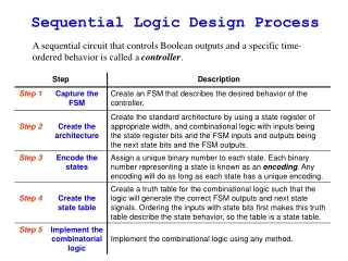
Sequential Switching Networks Sequential Circuit x1 Combinational Logic Delay = D z1 x2 z2 x3 z3 x4 z4 • z3 = F(x1, ... ,x4,z3,z4) • z3(t+D) = F(x1(t), ... ,x4(t),z3(t),z4(t)) • Observations: • z3 and z4 appear as both • inputs and outputs. • The “state” of variable z3 (or z4) at • time t+D depends on its value at • time t, i.e. z3(t+D) = F(z3(t)), • hence, circuit has memory. • z3(t) and z4(t) are called • state variables . • Sequential logic forms basis for building • "memory" into circuits. • Sequential logic is characterized by the • presence of feedback paths.
"1" "0" Delay=D Assuming D > 0 z(t+D) = x(t) z(t) if x(t) = 0 then z(t)=1 (stable state) if x(t) = 1 then z(t+D) = z(t) x(t) z(t) D D x z t z(t) Simple Sequential Circuits Cascaded Inverters: Static Memory Cell Another Example Observe that NAND gate with one input asserted acts as an inverter with respect to other input When x=1, equaivalent circuit Timing Waveform:
Inverter Chains and Ring Oscillators Inverter Chains Output high propagating thru this stage Odd # of stages leads to ring oscillator Snapshot taken just before last inverter changes Timing Waveform: tp = n D n = no. inverters
x(t) z(t) 0 X x R q q Q Q S R S Cross-Coupled NOR Gates Simple-Latch: two-inverter loop x=1 --> z=0 x=0 --> z=1 Problem: how can we insert x in the loop? Observation NOR gate with one input=0, acts as an inverter with respect to other input. Equivalent NOR circuit with two control inputs (R and S) to break or close the loop Alternative representation R: Reset input (R=1 --> Q=0) S: Set input (S=1 --> Q=1)
R=0 R=0 q=0 q=1 Q=1 Q=0 S=0 S=0 R=1-->0 R=1 q=0 q=0-->1-->0-->1-- 0-->1-->0-->1 0-->1-->0-->1 Q=0 S=1 Q=0-->1-->0-->1-- S=1-->0 The RS Latch • if R=S=0 then Q(t+D)=Q(t) (memory element) • if R=S=1 then q = Q = 0, which violates the inverter rule (q = 0, Q = 1) • if R and S chnage from 1-to-0 at precisely same moment, then RS latch • will oscillate (provided the NOR gate delays are perfectly matched)
State Behavior of RS Latch The response and transient behavior of the RS latch can be described using a state-diagram: 1- Nodes represent the unique states of the circuit 2- Arcs indicate state-transition under particular input combinations (arc labels). state 1 state 2 Truth Table Summary of R-S Latch Behavior state 0 Because of the resulting unstable behavior the combination R=S=1 is called the forbidden input for the RS latch. state 3
PS NS (q+, Q+) qQ SR SR SR SR 00 01 10 11 00 11 01 10 00 01 01 01 10 00 10 10 01 10 00 00 00 01 10 00 PS : present state NS: next state Q+ : Q(t+D) State-Diagrams and State Tables A state-table expresses the same information of the state-diagram in a tabular format Note the unstable behavior is now obvious from the continuous transition states 00 and 11 when SR changes from 11 to 00.
enabled when C=1 D Q q C Clk Enable D R q q RS Latch S Q C The D-Latch if C=1 then Q=D if C=0 then Q(t+D)=Q(t) Realization using an RS latch if C=0, then R=S=0 and Q(t+D)=Q(t) If C=1 and D=0 then R=1, S=0, and Q=0 if C=1 and D=1 then R=0, S=1, and Q=1 Note that input R=S=1 can not occur
Steup and Hold Times Clock: Periodic Event, causes state of memory element to change. Setup Time (Tsu): Minimum time before the clocking event by which the input must be stable Hold Time (Th) Minimum time after the clocking event during which the input must remain stable There is a timing "window" around the clocking event during which the input must remain stable and unchanged in order to be recognized Primitive Memory Elements: Latches: Continuously sample their inputs. Any change in the level of the inputs is propagated through to the outputs (level sensitive). Flip-Flops: Outputs change only with respect to the clock, normally the rising edge or the falling edges of the clock.
Reset Set Level Sensitive Latches RS latch with active-low inputs and active-low Enable Truth Table \enb S R Q+ 1 x x Q 0 0 0 Q 0 0 1 0 0 1 0 1 0 1 1 Unstable Timing Diagram:
Flip-Flops and Latches Edge triggered devices sample inputs on the rising or falling edge of the Clock or the Enable. Transparent latches sample inputs as long as the clock is asserted - output changes with input (after certain delay). 7474 Timing Diagram: 7476 Bubble here for negative edge triggered device Behavior is the same unless input changes occur while the clock is high
Flip-Flops vs. Latches Input/Output Behavior of Latches and Flipflops Type When Inputs are SampledWhen Outputs are Valid unclocked always propagation delay from latch input change level clock high propagation delay from sensitive (Tsu, Th around input change latch falling clock edge) positive edge clock lo-to-hi transition propagation delay from flipflop (Tsu, Th around rising edge of clock rising clock edge) negative edge clock hi-to-lo transition propagation delay from flipflop (Tsu, Th around falling edge of clock falling clock edge) master/slave clock hi-to-lo transition propagation delay from flipflop (Tsu, Th around falling edge of clock falling clock edge)
Flip-Flops: Typical Timing Specifications 74LS74 Positive Edge Triggered D Flipflop • Setup time • Hold time • Minimum clock width • Propagation delays (low to high, high to low, max and typical) All measurements are made from the clocking event that is, the rising edge of the clock
Latches: Typical Timing Specifications 74LS76 Transparent Latch • Setup time • Hold time • Minimum Clock Width • Propagation Delays: high to low, low to high, maximum, typical data to output clock to output Measurements from falling clock edge or rising or falling data edge
q q q R Q S R S Designing Latches Derived K-Map: RS Latch Truth Table: Next State = F(S, R, Current State) Characteristic Equation: q(t+D)=s(t)+R(t)q(t) or q+=s + Rq Compare to previous NOR implementation
J Q D K D-Latch C enb The JK Latch The JK latch eliminates the forbidden state of the RS latch Basic principle: use output feedback to guarantee that R=S=1 never occurs J=K=1 yields toggle (q+ = Q) Characteristic Equation: Q+ = Q K + Q J
PS NS (q+, Q+) PS NS (q+, Q+) q SR SR SR SR 00 01 10 11 0 0 0 1 x 1 1 0 1 x Q Q 0 1 x q JK JK JK JK 00 01 10 11 0 0 0 1 1 1 1 0 1 0 Q Q 0 1 Q JK=00 , 10 JK=01 , 11 J K Q+ 0 0 Q 0 1 0 1 0 1 1 1 Q Q=1 Q=0 JK=10 , 11 JK=00, 01 JK Latches Simplified State-Tables
Reset Set Toggle Race Condition From JK Latch to JK Flip-Flop JK Latch: Race Condition • Ideally, the Latch should toggle only once when JK=11. • Because of latch transparency, race conditions cause continuous toggrling. • Toggle Correctness: Single State change per clocking event • Solution: Master-Slave Flipflop
Master Stage Slave Stage Sample inputs while clock low Sample inputs while clock high Master-Slave JK Flip-Flop Break feedback path, by dividing operation in two time periods (clock-high and clock-low) Correct Toggle Operation
T Q Q+ 0 0 0 0 1 1 1 0 1 1 1 0 T Q+ 0 Q 1 Q T J K Q+ 0 0 0 q 1 1 1 Q D Q T D flipflop T J Q JK flipflop C C K The Toggle (T) FlipFlop State table T Q or T flipflop C T-FF can be realized using a JK-FF Verification: J=K=T q+ = tQ+Tq T-FF can be realized using a D-FF
D Clk Q Edge-Triggered FlipFlops Example: • Negative edge-triggered D flipflop • Flipflop state changes right after the falling edge of the clock • 4-5 gate delays (longer than latches) • Setup and Hold times are necessary for correct operation Characteristic equation Q+ = D
Edge-Triggered D FlipFlopk Step-by-step analysis When clock goes from high-to-low data is latched When clock is low data is held
Positive and Negative Edge Triggered FlipFlops Timing Diagram Positive Edge Triggered Inputs sampled on rising edge Outputs change after rising edge Negative Edge Triggered Inputs sampled on falling edge Outputs change after falling edge
Comparison R-S Clocked Latch: used as storage element in narrow width clocked systems its use is not recommended! however, fundamental building block of other flipflop types J-K Flipflop: versatile building block can be used to implement D and T FFs usually requires least amount of logic to implement ƒ(In,Q,Q+) but has two inputs with increased wiring complexity because of 1's catching, never use master/slave J-K FFs Use edge-triggered varieties D Flipflop: minimizes wires, much preferred in VLSI technologies simplest design technique best choice for storage registers T Flipflops: don't really exist, constructed from J-K FFs usually best choice for implementing counters Asynchronous Preset and Clear inputs are highly desirable!
D Q+ 0 0 1 1 Q Q+ D 0 0 0 0 1 1 1 0 0 1 1 1 Q Q+ T 0 0 0 0 1 1 1 0 1 1 1 0 T Q+ 0 q 1 Q FlipFlop Excitation Tables Useful Design Tool: For each state-transition, the excitation table lists the required input combination(s) 1. D FlipFlop D Q D flipflop C Transition Table q+ = d Excitation Table 2. T FlipFlop T Q T flipflop C Transition Table q+ = tQ+Tq Excitation Table
RS=00,01 RS=00,10 RS= 01 Q=0 Q=1 RS=10 R Q SR flipflop Clk S JK= 10, 11 Q=0 Q=1 JK= 01, 11 J Q JK flipflop Clk K FlipFlop Excitation Tables 1. SR FlipFlop q+ = s + Rq R S Q+ 0 0 Q 0 1 1 1 0 0 1 1 forbid Q Q+ R S 0 0 X 0 0 1 0 1 1 0 1 0 1 1 0 X Transition Table Excitation Table JK=00,10 JK=00,01 1. JK FlipFlop q+ = jQ + Kq R S Q+ 0 0 q 0 1 1 1 0 0 1 1 Q Q Q+ J K 0 0 0 X 0 1 1 X 1 0 X 1 1 1 X 0 Transition Table Excitation Table
g CL x Q x Q y CL y h Conversion Between FlipFlop Types Procedure uses excitation tables Method: to realize a type A flipflop using a type B flipflop: 1. Start with the K-map or state-table for the A-flipflop. 2. Express B-flipflop inputs as a function of the inputs and present state of A-flipflop such that the required state transitions of A-flipflop are reallized. Type B Type A 1. Find Q+ = f(g,h,Q) for type A (using type A state-table) 2. Compute x = f1(g,h,Q) and y=f2(g,h,Q) to realize Q+.
Conversion Between FlipFlop Types Example: Use JK-FF to realize D-FF 1) Start transition table for D-FF 2) Create K-maps to express J and K as functions of inputs (D, Q) 3) Fill in K-maps with appropriate values for J and K to cause the same state transition as in the D-FF transition table D Q Q+ J K 0 0 0 0 X 0 1 0 X 1 1 0 1 1 X 1 1 1 X 0 State-Table e.g. when D=Q=0, then Q+= 0 the same transition Q-->Q+ is realize with J=0, K=X
J J K Q Q+ D T 0 0 0 0 0 0 0 0 1 1 1 0 0 1 0 0 0 0 0 1 1 0 0 1 1 0 0 1 1 1 1 0 1 1 1 0 1 1 0 1 1 1 1 1 1 0 0 1 Q D K DFF C Clk J Q T K T-FF C Clk J J JK JK 00 01 11 10 00 01 11 10 Q Q 0 0 0 1 1 0 0 0 1 1 1 1 0 0 1 1 0 1 1 0 K K d= jQ + Kq t= jQ + kq Conversion Between FlipFlops Another Example: Implement JK-FF using a D-FF
PRESET T Q Clk CLEAR SET 1 0 S Q 1 D Q T 0 C Q R Clk 1 CLR 0 Asynchronous Inputs PRESET and CLEAR: asynchronous, level-sensitive inputs used to initialize a flipflop. PRESET, CLEAR: active low inputs PRESET = 0 --> Q = 1 CLEAR = 0 --> Q = 0 LogicWorks Simulation
Proper Cascading of Flipflops Serial connection of positive edge-trigerred flipflops 1. on rising efge of CLK, FF1 reads Q0, and FF0 reads IN 2. during clock period FF1 performs Q1 <-- Q0, and FF0 performs Q0 <-- IN FF0 FF1 Shift-register Correct Operation, assuming positive edge triggered FF