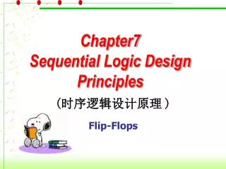
Chapter7 Sequential Logic Design Principles
Chapter7 Sequential Logic Design Principles. ( 时序逻辑设计原理 ). Flip-Flops. CLK. Flip-Flops ( 触发器 ). Positive-Edge Rising-Edge. Negative-Edge Falling-Edge. Change its outputs only at the Rising or Falling Edge of a controlling CLK signal. Flip-Flop. Classified by Function

Chapter7 Sequential Logic Design Principles
E N D
Presentation Transcript
Chapter7 Sequential Logic Design Principles (时序逻辑设计原理) Flip-Flops
CLK Flip-Flops (触发器) Positive-Edge Rising-Edge Negative-Edge Falling-Edge Change its outputs only at the Rising or Falling Edge of a controlling CLK signal.
Flip-Flop • Classified by Function • D Flip-Flop、S-R Flip-Flop • J-K Flip-Flop 、T Flip-Flop • Classified by Structure • Master/Slave Flip-Flop (主从结构触发器) • Edge-Triggered Flip-Flop(边沿触发器) • Other TypesFlip-Flop • Flip-Flopwith enable、Scan Flip-Flop…
Master Slave Qm D D Q C Q D Q C Q Q QL CLK Edge-Triggered D Flip-Flops ——Master / Slave CLK=0时, 主锁存器工作,接收输入信号 Qm = D 从锁存器不工作,输出 Q 保持不变 主锁存器不工作,Qm 保持不变 从锁存器工作,将 Qm 传送到输出端 CLK=1时,
Qm master slave Qm D D Q C Q D Q C Q Q QN CLK CLK D Qm Q
Logic symbol D CLK Q QN Function table D Q CLK Q 0 0 1 1 1 0 X 0 Hold X 0 Hold Dynamic-input indicator 表示边沿触发特性 CLK D Q The state changed only at the trigger time !
Q CLK CLK D D Q Dlatch ——电平有效 Dfilp-flop —— 边沿有效
tpHL(CQ) tpLH(CQ) tsetup 建立时间 thold 保持时间 Time behavior of DFlip-Flop • Setup time(建立时间,输入信号先于时钟到达的时间) • Hold time(保持时间,有效时钟沿后输入信号保持的时间) • Propagation deay(CLKQ) D CLK Q
PR_L D Q PR D Q CLK Q CLR QL CLR_L CLK Positive-Edge-Triggered D Flip-Flopwith preset and clear PR(preset)、CLR(clear) 相当于: S(set) 、 R(reset) 通常用于初始化电路状态、测试等
CLK PR_L CLR_L QN Time behavior of a positive-edge-triggered D flip-flop with preset and clear
Commercial circuit for a positive-edge-triggered D flip-flop 74LS74 商用电路(图7-20) 维持阻塞结构D触发器
master slave Qm D D Q C Q D Q C Q Q D D Q C Q D Q C Q Q QN QN CLK CLK D Q CLK Q Positive-edge-triggered 正边沿触发 Negative-Edge-Triggered D Flip-Flop Negative-edge-triggered 下降沿有效
2-input multiplexer D EN D Q CLK Q Q QN D Q EN CLK Q CLK 逻辑符号 D Flip-Flop with Enable EN is asserted(=1) 选择外部D输入 ENis negated(=0) 选择触发器当前的输出
Dynamic DFF Store data in input comparator of INV Simple , cheap and fast State must be keep refresh
D TE TI CLK D Q Q TE D Q CLK Q Q QL TI CLK Scan Flip-Flop (扫描触发器) Function table:P536Fig.7-22 Logic Symbol • TE = 0 normal mode Q=D • TE = 1 test mode Test enable input Test input
TIN TO CLK TE • TE = 0 normal mode • TE = 1 test mode • 每个触发器的输出端Q都与后一个触发器的TI端连接 • TIN 端扫入一组测试向量(需若干个时钟触发沿) • 再经过若干个时钟的正常操作(TE=0) • 可以在TO端观察(扫出)电路的新状态
功能表 J K Q 0 0 0 1 1 0 1 1 保持 清0 置1 翻转 JKFlip-flop
状态转移真值表 Qn+1 JK 00 01 11 10 J K Qn Qn+1 Qn 0 1 1 0 0 1 0 0 0 0 0 1 0 1 0 0 1 1 1 0 0 1 0 1 1 1 0 1 1 1 0 1 0 0 1 1 1 0 维持 0 1 0 1 清0 特征方程 置1 Q* = J·Q’ + K’·Q 翻转 J-K Flip-Flop
TFlip-flop T(toggle)
T Q CLK Q EN Q T Q 有使能端的T触发器: Q* = EN·Q’ + EN’·Q Q Q T Important Note 教材中的T触发器 • 以后我们提到的T触发器均指的是 特征方程:Q* = Q’ T 触发器的特征方程为:Q* = T·Q’ + T’·Q 当T=1,触发器的特征方程为:Q* = Q’ (也称为T’触发器)
Summary of Latches and Flip-flops • 锁存器和触发器 —— 电平有效和边沿有效的区别 • 按照逻辑功能的不同特点,通常可分为 • S-R触发器(锁存器) • D触发器(锁存器) • J-K触发器 • T触发器 每种触发器的 功能表 特征方程 状态图
功 能 表 S R Q 时钟S-R锁存器 基本S-R锁存器 维持 清 0 置 1 0* 0 0 0 1 1 0 1 1 S C R 功 能 表 Q Q S R Q S Q R Q 0 0 0 1 1 0 1 1 维持 清 0 置 1 1* (或非门) 主从S-R触发器 SL RL Q S Q R Q S C R Q 1 1 1 0 0 1 0 0 维持 清 0 置 1 1* Q (与非门) S-R Flip-Flops (Latches) 0 1* 0
低电平有效S-R锁存器 状态转移真值表 Qn+1 S_LR_L 00 01 11 10 S_L R_L Qn Qn Qn+1 0 1 0 1 0 0 0 0 0 0 1 0 1 0 0 1 1 1 0 0 1 0 1 1 1 0 1 1 1 1* 1* 1 1 0 0 0 1 1 1 0 特征 方程 Q* = S+ R’·Q S·R=0(约束条件) Q* = S_L’ + R_L·Q = S+ R’·Q 约束条件:S_L + R_L = 1 S’+R’=1 S·R=0
功能表 特征方程 Q* = S+ R’·Q S·R=0(约束条件) S R Q 维持 0 1 1* 0 0 0 1 1 0 1 1 S=1,R=0 S=X R=0 S=0 R=X 0 1 S=0,R=1 S-R Flip-Flops (Latches) 状态图
D=1 D=0 D=1 0 1 D=0 D Flip-Flops (Latches) 特征方程:Q* = D 状态图 有使能端得D触发器:Q* = EN·D + EN’·Q
状态转移真值表 Qn+1 JK 00 01 11 10 J K Qn Qn+1 Qn 0 1 1 0 0 1 0 0 0 0 0 1 0 1 0 0 1 1 1 0 0 1 0 1 1 1 0 1 1 1 0 1 0 0 1 1 1 0 维持 0 1 0 1 清0 特征方程 置1 Q* = J·Q’ + K’·Q 翻转 J-K Flip-Flop
功能表 J K Q* J=0 K=X J=X K=0 维持 清 0 置 1 翻转 0 0 0 1 1 0 1 1 特征方程 J=1,K=X Q* = J·Q’ + K’·Q 0 1 J=X,K=1 J-K Flip-Flop 状态图
T Q CP Q Tflip-flop 特征方程:Q* = T·Q’ + T’·Q
Q* = S+ R’·Q S·R=0(约束条件) • S-R flip-flop • J-Kflip-flop Q* = J·Q’ + K’·Q • Dflip-flop Q* = D Q* = T·Q’ + T’·Q • T flip-flop Flip-Flops Summary Characteristic Equations D flip-flopwith enable:Q* = EN·D + EN’·Q
Using DFlip-flop to build S-R Flip-flop J-K Flip-flop T Flip-flop Using J-K Flip-flop to build S-R Flip-flop D Flip-flop T Flip-flop Conversions between different flip-flop types
Q Q D QN T' Q >CLK Q Q =1 D T QN CP Q >CLK & J & Q Q D & K & QN Q CLK >CLK Convert D flip-flop to other flip-flop DFlip-flop toT’ Flip-flop : D = Q’ DFlip-flop toT Flip-flop : D = Q ⊕ T D Flip-flop toJK Flip-flop : D = J • Q’ + K’ • Q
D J Q Q CLK >CLK QN Q 1 K T J Q Q CP >CLK QN Q K 1 J Q Q CP >CLK QN Q K Convert JK flip-flop to other flip-flop JK Flip-flop toD Flip-flop: J = D K = D’ JK Flip-flop toTFlip-flop: J = K = T JK Flip-flop toT’ Flip-flop: J = K = 1
Q Q =1 T D QN CP Q >CLK T = D⊕Q & J & Q Q T K & QN Q CLK >CLK T = J •Q + K •Q Convert T flip-flop to other flip-flop T Flip-flop toD Flip-flop: TFlip-flop toJK Flip-flop:
Register design module latch (d,c,q); input d,c; output q; assign q = (c ? d:q); endmodule
Always block and Variable … reg[7:0] f ; … always @ (posedge clk) begin variable assignment; end Variable: must be reg , assigned in always block !
Always block and Variable Variable: Operational result , must be reg , may be stored in register, assigned in always block. Blocking assignment: sequential design f <= x & y; Nonblocking assignment: combinational design f = x & y;
Register design module dff (clk,d,q,qn); input clk,d; output q,qn; reg q,qn; always @ (posedge clk) begin q <= d ; end always @ (q) begin qn = ~q; end endmodule
Register design module reg8 (clk,clr,d,q); input clk,clr; input[7:0] d; output[7:0] q; reg[7:0] q; always @ (posedge clk) begin if (clr==1'd1) q<= 8'd00000000; else q<= d;end endmodule
7.4 7.5 7.6 7.7 7.8 7.10 Homework