Sequential Logic Design
Sequential Logic Design. CT101 – Computing Systems Organization. Contents. Basic Sequential Components FlipFlop , Latches, Counters Programmable Logic Devices PLD, PLA, CPLDs & FPGAs Finite State Machine Model Generic Model Synchronous Model Mealy & More FSMs. Overview.

Sequential Logic Design
E N D
Presentation Transcript
Sequential Logic Design CT101 – Computing Systems Organization
Contents • Basic Sequential Components • FlipFlop, Latches, Counters • Programmable Logic Devices • PLD, PLA, CPLDs & FPGAs • Finite State Machine Model • Generic Model • Synchronous Model • Mealy & More FSMs
Overview • The most fundamental sequential components are the latch and flip-flop • They store one bit of data and make it available to other components • The main difference between a latch and a flip-flop is that the first are level triggered and the latter are edge triggered • Flip-flops and latches have a clock input
Clock • It is usually derived from an oscillator or other circuitry that alternates its output between 1 and 0 • It is used to synchronize the flow of data in a digital system
D flip-flop • Flip-flop: • One data input D • When the clock input changes from 0 to 1 (positive edge), the data on the D input is loaded • The data is made available via output Q and its complement via Q’ • Some variations have also a load signal (LD) that has to be high (active) in order for data to be loaded into the flip-flop
D latch • Positive level triggered latch • It loads data as long as both its clock and load signals are 1. If both are one, the value of data D is passed to the Q output. If D changes while clock and load are 1, then the output changes accordingly • If either the clock or load signals go to 0, the Q value is latched and held
D latch with clear/set capabilities • Some variants of D latch and flip-flops have asynchronously set and clear capabilities – they can be set and clear regardless of the value of the other inputs to the latch (including the clock and load inputs)
SR latch • The S input sets the latch to 1 and the R input resets the latch to 0 • When both S and R are 0 the output remains unchanged • Doesn’t have a clock input • Only sequential component without a clock input • The output of the latch is undefined when both the S and R are 1; the designer has to ensure that S and R inputs are never set to 1
JK flip-flop • Resolves the problem of undefined outputs associated with SR latch • J=1 sets the output to 1 and K=1 resets the output to 0. JK=11 inverts the stored current value of the output • It is often used instead of SR latch
T (toggle) flip-flop • The T input doesn’t specify a value for its output, it specifies only whether or not the output should be changed • On the rising edge of the clock, if T = 0 then the output of the flip-flop is unchanged; if T=1, the output is inverted.
Observations • All of the flip-flops and latches shown so far are positive edge triggered or positive level triggered. They also have active high load, set and clear inputs. • It is possible for those components to be negative edge triggered or negative level triggered and have active low control signals as well. • Flips-flops and latches can be combined in parallel to store data with more than one bit
4 bit D flip-flop • Control signals are tied together • Act as one unified data register • They usually output only the data (not the complement of the data as the 1 bit flip-flops)
Counters • Store a binary value and when signaled to do so, it increments or decrements its value • Can be loaded with an externally supplied value INC=1 Current Counter Value: 1111 Next Counter Value: 0000
Up/down counter with parallel load • Ability to load external data as well as count • Down counter decrements its value rather than increment and generates a borrow rather than a carry out • Up/down counter can do both operations according with the signal U/D’
Shift Registers • Can shift its data one bit position to the right or left • It is useful for hardware multipliers/dividers • It may shift left, right or both directions under certain control conditions (like the up/down counter)
Programmable Logic Devices • Most of the circuits presented so far are available on a TTL IC chip. Circuits can be constructed using these chips and wiring them together • An alternative to this method would be to program all the components into a single chip, saving wiring, space and power • One type of such device is PLA (Programmable Logic Array) that contains one or more and/or arrays.
PLA • The inputs and their complements are made available to several AND gates. • An X indicates that the value is input to the AND gate • The output from the AND gates are input into the OR gates, which produce the chip’s outputs • Functions: • b = X2’ + X1’X0’+X1X0 • c = X2 + X1’ + X0
PAL • Programmable Array of Logic – its OR blocks are not programmable • Certain AND gates serve as input to specific OR gates • Same b and c function implementation: b = X2’ + X1’X0’+X1X0 c = X2 + X1’ + X0 • PLA and PAL are limited because they can implement only combinatorial logic, they don’t contain any latches nor flip-flops
PLD • Programmable Logic Device is a more complex component that is needed to realize sequential circuits • It is usually made up of logic blocks with the possibility to interconnect them. • Each logic bloc is made out of macro cells, that may be equivalent to a PAL with an output flip-flop • The input/output pins of an PLD can be configured to the desired function (unlike for PLA or PAL, where they are fixed) • Used in more complex design than the PAL or PLA
CPLDs • Array of PLDs • Has global routing resources for connections between PLDs and between PLDs to/from IOs
FPGAs • Field Programmable Gate Array is one of the most powerful and complex programmable circuit available • Contain an array of cells, each of which can be programmed to realize a function • There are programmable interconnects between the cells, allowing connect to each other • Includes flip-flops allowing the design and implementation of complex sequential circuit on a chip (of a complexity of a processor) • Often contains the equivalent of 100k to a few million simple logic gates on a single chip
FPGAs • Configuration Memory • Programmable Logic Blocks (PLBs) • Programmable Input/Output Cells • Programmable Interconnect Typical Complexity = 5M - 100M transistors
Basic FPGA Operation 1110011010001000100101010001011100010100101010101001001000100010101001001001100100100001111000110010100010000110010001010001001001001000101001010101001001001010001010010100010100101001000100101010111010101010101010101010101111011111000000000000001101001111100001001110000011100100101000000001111100100100010100111001001010000111100011100010010101010101010101010010100101010100100101010101010101001001001 • Load Configuration Memory • Defines system function (Input/Output Cells, Logic in PLBs, Connections between PLBs & I/O cells) • Changing configuration memory => changes system function • Can change at anytime • Even while system function is in operation • Run-time reconfiguration (RTR)
LUT/ RAM FF LUT/ RAM FF LUT/ RAM FF LUT/ RAM FF PLB architecture Programmable Logic Blocks • PLBs can perform any logic function • Look-Up Tables (LUTs) • Combinational logic • Memory (RAM) • Flip-flops • Sequential logic • Special logic • Add, subtract, multiply • Count up and/or down • Dual port RAM • #PLBs per FPGA: 100 to 500,000
wire B wire C wire A wire A wire B wire B output wire B wire A wire A configuration memory element break-point PIP multiplexer PIP cross-point PIP Programmable Interconnect • Wire segments & Programmable Interconnect Points (PIPs) • cross-point PIPs – connect/disconnect wire segments • To turn corners • break-point PIPs – connect/disconnect wire segments • To make long and short signal routes • multiplexer (MUX) PIPs select 1 of many wires for output • Used at PLB inputs • Primary interconnect media for new FPGAs
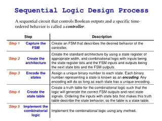
FSM Overview • Finite State Machine is a tool to model the desired behavior of a sequential system. • The designer has to develop a finite state model of the system behavior and then designs a circuit that implements this model • A FSM consists of several states. Inputs into the machine are combined with the current state of the machine to determine the new state or next state of the machine. • Depending on the state of the machine, outputs are generated based on either the state or the state and inputs of the machine.
FSM Structure • X represents the range of possible input values (2n) • Y represents the range of output values (2m) • Q represents the range of the possible states of the system (2k) • Transfer functions: • f: X x Q -> Y • g: X x Q -> Q
FSM Representation • FSM = (X, Y, Q, f, g) • If there is no state in the Q range (Q≡Ø, the circuitry has no history), then: • g: X x Ø->Ø, there is no state transition function • f: X x Ø -> Y is becoming f: X -> Y • In this case, the FSM is equivalent to an CLC • FSM| Q≡Ø = CLC = (X, Y, f)
Asynchronous vs. Synchronous • Async FSM – the next state becomes the present state after the delays through the delay elements • Sync FSM – obtained by replacing the delay elements di with memory elements (registers). • The wi bits of the next state will be written in the registers (memory elements) only on the clock (on edge or level) is applied.
Sync FSM with immediate outputs The FSM where the outputs, after they have been calculated, are used immediately (of course in the stable period of the state interval), is called an immediate state machine.
Sync FSM with delayed outputs The next state is assigned as present state on the next clock cycle. Similarly, we can proceed with the outputs, obtaining the delayed state machine. Each bit of the output is passed through a memory element.
FSM Example • Events: • Wake up at fixed time every day • Weekends: you don’t need alarm, so you wake up, turn off the alarm and resume sleep • FSM modeling this chain of events, with: • Three states: • Asleep • Awake but still in bed • Awake and up • Inputs: • Alarm • Weekday (determines you how to react to alarm) • Outputs: • Turn off the alarm
State tables • Similar to the truth table • Doesn’t contain the system clock when specifying its transitions (it is implicit that transitions occur only when allowed by clock) • Unless different stated, all the transitions are occurring on the positive edge of the clock
Alarm clock state table • When you are asleep and alarm goes on, you go from being asleep to being awaked in bed; you also turn off the alarm • The next two rows encode your actions: • You get up • You go back to sleep • This table doesn’t cover what you wouldn’t do…(i.e. if you are asleep and the alarm doesn't go off, you remain asleep, etc..)
Alarm clock state table • Covers all the cases • First row covers the situation you are asleep, the alarm doesn’t go off and you remain asleep • Last row covers the situation you are awake and up and you remain awake and up • The third row covers the case you are already up and the alarm goes off. You turn it off and remain Awake in bed
State diagram • Graphical representation of the state table • Each state is represented by a circle vertex • Each row of the state table is represented as a directed arc from present state vertex to the next state vertex • In this diagram, the outputs are associated with the states
Alternative state diagram • The outputs are associated with the arcs • An output of 1 represents that “turn off the alarm” is Yes • By convention , inputs which are don’t care and inactive outputs are not shown.
Mealy and Moore machines • Moore machine • Associates its outputs with states • The outputs are represented either within the vertex corresponding to a state or adjacent to the vertex • Mealy machine: • Associates its outputs with the transitions • In addition to the input values, each arc also shows the output values generated during the transition; the format of the label of each arc is Inputs/Outputs • Both can be used to represent any sequential system and each has its advantages.
Mealy FSM • Output is dependent on the inputs and the current state • Delayed output FSM implies the fact that the calculated output for an input applied at time t is assigned at time t+1. This is correct at an Mealy FSM
Moore FSM • Output is dependent only on the current state • Immediate Moore FSM: the output is obtained with a clock period delay, since the then the next state becomes present state • Delayed Moore FSM: the output is actually obtained with two clock period delay, because of the Registers Bank 2
Moore machine diagram • Self arcs can be missing (since it outputs are associated with the states and not with the arcs) • Offers a simpler implementation when the output values depend only on the state and not on the transitions • It is well suited for representing the control units of microprocessors
Mealy machine diagram • Self arcs must be shown (because the output values are shown on the arcs) • Can be more compact than Moore machine, especially when two or more arcs with different output values go into the same state
References • “Computer Systems Organization & Architecture”, John D. Carpinelli, ISBN: 0-201-61253-4