3.3 CMOS Logic
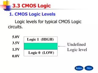
5.0V. Logic 1 (HIGH). 3.5V. Undefined Logic level. 1.5V. Logic 0 (LOW). 0.0V. Return. Next. 3.3 CMOS Logic. 1. CMOS Logic Levels. Logic levels for typical CMOS Logic circuits. V IN. Return. Back. Next. 3.3 CMOS Logic. 2. MOS Transistors.

3.3 CMOS Logic
E N D
Presentation Transcript
5.0V Logic 1 (HIGH) 3.5V Undefined Logic level 1.5V Logic 0 (LOW) 0.0V Return Next 3.3CMOS Logic 1. CMOS Logic Levels Logic levels for typical CMOS Logic circuits.
VIN Return Back Next 3.3CMOS Logic 2. MOS Transistors • A MOS transistor can be modeled as a 3-terminal device that acts like a voltage controlled resistance. • In digital logic applications, a MOS transistor is operated so its resistance is always either very high (and the transistor is “off”) or very low (and the transistor is “on”) .
drain gate + Vgs source - drain gate + Vgs source - Return Back Next 3.3CMOS Logic • n-channel MOS (NMOS) Increase Vgs→decrease Rds Normally, Vgs≥ 0 • Vgs=0 → Rds106 () • → I 10-6 (A) 0 • Vgs Vgs(th) → Rds 10 () << RL →VRds 0
source - Vgs + gate drain source - Vgs + gate drain Return Back Next 3.3CMOS Logic • p-channel MOS (PMOS) Decrease Vgs→decrease Rds Normally, Vgs 0 • Vgs=0 → Rds ≥ 106 () • Vgs Vgs(th) → Rds 10 () Switch Model
VDD=+5.0V VDD=+5.0V Q2 (PMOS) VOUT=H VIN=L VOUT VIN Q1 (NMOS) VDD=+5.0V VIN Q1 Q2 VOUT VOUT=L VIN=H 0.0(L) off on 5.0(H) Return Back Next 3.3CMOS Logic 3. Basic CMOS Inverter Circuit 5.0(H) on off 0.0(L)
VDD=+5.0V Q2 (PMOS) Z A Q1 (NMOS) Return Back Next 3.3CMOS Logic • CMOS inverter logical operation Truth table for CMOS inverter On when Vin is low. On when Vin is high.
VDD VDD VDD VDD VDD Z=H A=L Z=H Q2 Z=H Q4 A=L Z=L A=H B=L A=H B=H Z B=L B=H A Q1 B Q3 A Z B Return Back Next 3.3CMOS Logic 4. CMOS NAND Gates
VDD Q2 A B Q4 Z Q1 Q3 A Z B Return Back Next 3.3CMOS Logic 5. CMOS NOR Gates
VDD Q2 Q6 Q4 Z A Q1 B Q3 C Q5 Return Back Next 3.3CMOS Logic 6. Fan-In In principle, you could design a CMOS NAND or NOR gate with a large number of inputs. A 3-input CMOS NAND gate is showed in the figure. Why couldn't a CMOS gate has large number of inputs?
Return Back Next 3.3CMOS Logic • Fan-In A n-channel transistor has low “on” resistance than a p-channel transistor. As a result, a k-input NAND gate is generally faster than a k-input NOR gate. The number of inputs that a gate can have in a particular logic family is called the logic family’s fan-in. The fan-in of CMOS gates is typically 4 for NOR gates and 6 for NAND gates. Why is the fan-in of CMOS gates for NOR gates less than the ones for NAND gates?
I1 I1 I2 I2 I3 I3 I4 I4 I5 I5 OUT OUT I6 I6 I7 I7 I8 I8 Return Back Next 3.3CMOS Logic • Fan-In As the number of inputs is increased, designers of CMOS gate circuits may compensate by increasing the size of the series transistors to reduce their resistance and the corresponding switching delay.
Return Back Next 3.3CMOS Logic 7. Noninverting Gates (P93) • AND Gate • OR Gate 8. CMOS AND-OR-INVERT Gate (P94) 9.CMOS OR-AND-INVERT Gate (P95)
Typical input-output transfer characteristic of a CMOS inverter Vout 5.0 HIGH 3.5 undefined 1.5 LOW 1.5 3.5 5.0 Vin HIGH undefined LOW Return Back Next 3.3CMOS Logic 10. CMOS Steady-State Electrical Behavior
Vcc VOHmin High-state DC noise margin HIGH 0.7Vcc VIHmin ABNORMAL VILmax 0.3Vcc Low-state DC noise margin LOW VOLmax 0 Return Back Next 3.3CMOS Logic • Logic Levels and Noise Margins • VOHmin: The minimum output voltage in the HIGH state. VOHmin=VCC–0.1V • VOLmax: The maximum output voltage in the LOW state. VOLmax=ground+0.1V
Return Back Next 3.3CMOS Logic • VIHmin: The minimum input voltage guaranteed to be recognized as a HIGH. VIHmin=0.7VCC • VILmax: The maximum input voltage guaranteed to be recognized as a LOW. VILmax=0.3VCC • DC noise margin: is a measure of how much noise it takes to corrupt a worst-case output voltage into a value that may not be recognized properly by an input. HIGH-state DC noise margin:VOHmin -VIHmin LOW-state DC noise margin: VILmax -VOLmax
Return Back Next 3.3CMOS Logic • IIH: The maximum current that flows into the input in the HIGH state. • IIL: The maximum current that flows into the input in the LOW state. Regardless of the voltage applied to the input of a CMOS device, only the leakage current of the transistors connected to input. This is in sharp contrast to bipolar logic circuits like TTL oe ECL, whose inputs consume significant current (and power) in one or both states.
Return Back Next 3.3CMOS Logic • Circuit Behavior with Resistive Loads • Resistive Loads: (P102). • IOLmax: The maximum current that the output can sink in the LOW state while still maintaining an output voltage no greater than VOLmax. • IOHmax: The maximum current that the output can sink in the HIGH state while still maintaining an output voltage no less than VOHmin.
Return Back Next 3.3CMOS Logic • Fanout : The fanout of a logic gate is the number of inputs that the gate can drive without exceeding its worst-case loading specifications. • DC Fanout : the output in a constant state (HIGH or LOW). • Overall Fanout : is the minimum of the HIGH-state and LOW-state fanouts.
tf tr VIHmin VILmax tf tr Return Back Next 3.3CMOS Logic 11. CMOS Dynamic Electrical Behavior • Transition Time : The amount of time that output of a logic circuit takes to change from one state to another. (a) ideal case (b) approximation (C) actual case
Return Back Next 3.3CMOS Logic • Rise time(tr) : the amount of time an output voltage takes to pass through the “undefined” region from LOW to HIGH. • Fall time(tf) : the amount of time an output voltage takes to pass through the “undefined” region from HIGH to LOW. The rise and fall times of a CMOS output depend mainly on two factors, the “on” transistor resistance and the load capacitance.
tpLH tpHL Return Back Next 3.3CMOS Logic • Propagation Delay : the amount of time that it takes for a change in the input signal to produce a change in the output signal. • tpHL: The time between an input change and the corresponding output change when the output is changing from HIGH to LOW. • tpLH: The time between an input change and the corresponding output change when the output is changing from LOW to HIGH. Propagation delays for a CMOS inverter
50% VIH 50% VOH tpHL tpLH Return Back Next 3.3CMOS Logic Propagation delays for a CMOS inverter measured at midpoints of transitions • Power Consumption • Static power dissipation: The power consumption of a CMOS circuit whose output is not changing.
Return Back Next 3.3CMOS Logic Most CMOS circuits have very low quiescent power dissipation. This is what makes them so attractive for laptop computers and other low-power application. • Dynamic power dissipation: The power consumption of a CMOS circuit whose output is changing. It’s significant. PT: The circuit’s internal power dissipation due to output transitions.CPD: The power-dissipation capacitance. f : The transition frequency of the output signal.
Return Back Next 3.3CMOS Logic PL:the total amount of power dissipated by charging and discharging CL. CL: capacitive load on the output. The total dynamic power dissipation PD of a CMOS circuit is the sum of PT and PL. Based on this formula, dynamic power dissipation is often called CV2fpower.
Return Back Next 3.3CMOS Logic Notice (1) The output voltage will move away from the power-supply rail with nonideal inputs. (2) A slightly overloaded circuit will fail. Loading an output beyond its rated fanout will make the output voltage(VOL) increase beyond VOLmax in the LOW state, and the output voltage(VOH) fall bellow VOHmin in the HIGH state, and propagation delay to the output increase beyond specification, and out rise and fall times increase beyond specification, and the operating temperature of the device increase.
A F B C F A B +5V C 1k 1k F C A B Return Back Next 3.3CMOS Logic (3) An unused inputs can be tied to another. An unused AND or NAND input can be tied to logic 1. An unused OR or NOR input can be tied to logic 0. pull-up resistor pull-down resistor
Return Back Next 3.3CMOS Logic A pull-up or pull-down resistor is usually used. The resistor value is typically in the range 1-10k. Such a single resistor can serve multiple unused inputs. It is also possible to tie unused inputs directly to the appropriate power-supply rail. Unused CMOS inputs should never be left unconnected (or floating). Why?
Return Back Next 3.3CMOS Logic (4) Systems that use CMOS circuits require decoupling capacitors between VCC and ground. (5) ESD(Electro-Static Discharge) may damage the insulation between an input transistor’s gate and source and drain, causing a short-circuit between the device’s input and output.
EN_L=0 EN_L A B A B EN_L=1 EN=1 EN A B EN=0 Return Back Next 3.3CMOS Logic 12. Transmission Gates How can you create a 2-input multiplexer using transmission gates? (P123)
VOUT VT- VT+ 5.0 VIN 5.0 2.1 2.9 Return Back Next 3.3CMOS Logic 13. Schmitt-Trigger Inputs Voltage of hysteresis =VT+-VT-
VCC VCC EN VCC VCC C C EN EN A OUT C C EN EN OUT OUT D D A OUT OUT A D D A A B EN A B C D Q1 Q2 OUT L L H H L off off Hi-Z L H H H L off off Hi-Z H L L H H on off L H H L L L off on H Return Back Next 3.3CMOS Logic 14. Three-State Outputs
VCC Z Q2 A B Q1 Q2 Z L L off off open L H off on open H L on off open H H on on L A B Q1 VP RP A Z A B RL Z B Return Back Next 3.3CMOS Logic 15. Open-Drain Outputs Pull-up resistor
VP RP A Z=VOHmin B ILH IOHmin RL VP RP A Z=VOHmin ILL IOLmax B RL Return Back Next 3.3CMOS Logic • Pull-up resistor calculation Open-drain gates can be useful in driving light-emitting diodes (LEDs) and other devices; performing wired logic; and driving multisource buses.
Numeric function designator Alphabetic family mnemonic prefix Return Back Next 3.3CMOS Logic 16. CMOS Logic Families The first commercially successful CMOS family was 4000-series CMOS. 74FAMnn
Return Back 3.3CMOS Logic • HC: High-speed CMOS • HCT: High-speed CMOS, TTL compatible • VHC: Very High-speed CMOS • VHCT: Very High-speed CMOS, TTL compatible Electrical characteristics of the HC, HCT, VHC, and VHCT are different. They are summarized on page 137-144 in the text-book.