Advancements in Lithography and Process Improvement for Advanced CMOS Projects
This project focuses on enhancing lithography processes in semiconductor manufacturing, covering a wide range of topics. Key areas include the optimization of op-amp design, the evaluation of resist trimming recipes on LAM 490, and CMP techniques for STI and multilayer metals. Additional evaluations include nitride deposition and etch uniformity, along with improved resist coating methods. Significant findings involve aluminum deposition rates and incorporating BF2 implant in MESA for advanced CMOS processes. The research also encompasses testing of SUB-CMOS productions from ASML steppers.

Advancements in Lithography and Process Improvement for Advanced CMOS Projects
E N D
Presentation Transcript
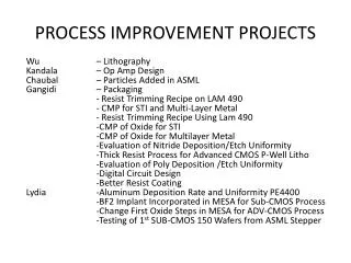
PROCESS IMPROVEMENT PROJECTS Wu – Lithography Kandala – Op Amp Design Chaubal – Particles Added in ASML Gangidi – Packaging - Resist Trimming Recipe on LAM 490 - CMP for STI and Multi-Layer Metal - Resist Trimming Recipe Using Lam 490 -CMP of Oxide for STI -CMP of Oxide for Multilayer Metal -Evaluation of Nitride Deposition/Etch Uniformity -Thick Resist Process for Advanced CMOS P-Well Litho -Evaluation of Poly Deposition /Etch Uniformity -Digital Circuit Design -Better Resist Coating Lydia -Aluminum Deposition Rate and Uniformity PE4400 -BF2 Implant Incorporated in MESA for Sub-CMOS Process -Change First Oxide Steps in MESA for ADV-CMOS Process -Testing of 1st SUB-CMOS 150 Wafers from ASML Stepper