Mid - Presentation
This presentation outlines the FPGA configuration process using FLASH memory, detailing the project goals, architecture, and implementation strategies. It describes the need for FPGA settings, emphasizing the advantages of using FLASH, including reduced space and power consumption. The project focuses on configuring system components, establishing robust data structures for storage and transmission, and enabling host communication via UART. Additionally, the simulation models and the development progress are outlined, along with the GUI testability aspects.

Mid - Presentation
E N D
Presentation Transcript
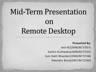
Mid - Presentation FPGA Setting Using Flash Dor Obstbaum Kami Elbaz Advisor: Moshe Porian August 2011
Content • Introduction • Project Goals • Requirements • Top level design • Project progress • Architecture & Micro Architecture • Simulations • Next steps • Testability & GUI • Schedule
Why do we need FPGA setting using FLASH? FLASH FPGA Client Client Generic! Client HOST Less space Software Independent Less power
Project goals • Configure system components using data stored in FLASH. • Implementing a data structure that will be used for data storage in FLASH and for data transmission to clients. • Setting an option for a host to read data from FLASH and write new data to it. • Implementing strong debugging capabilities.
Requirements • VHDL Implementation • DE2 development board that features an Altera Cyclone II FPGA • FPGA – Host communication via UART protocol • Internal communication via Wishbone protocol
MDWM FSM Wishbone MasterFSM
Simulations Simulation model • Simulation Plan: • Building a simulation model • Launching signals from a test file and observing the results • Simulations list: • - Configuration of a single client • - Configuration of 2 clients • - Minimum data length configuration • - Configuration of 2 clients twice • - Reading clients values • - Write to client, read value, write again.
Tx path Read data from client UART TX CRC FIFO WB Slave Wishbone to message encoder DATA Message encoder WB Master Operate the client RAM
For example: the TX receive request to read data from one client: Wishbone to Message encoder FSM: Waiting to the data Characteristic to be valid Update the outputs to the message encoder Valid_data_s = 0 Character update idel Valid_data_s = 1 Waiting for the data Storage in the client Pure_data_valid=‘0’ Wait for ack Data transmit via WB intercon to the unit, Byte by Byte Pure_data_valid= ‘1’ End transaction Transmit data temp_len != 0 Update the data output to the RAM, Finale state, after LENGTH byte of data was successfully transmit temp_len = 0
Wait Client Sys_clk Timer 100 MHz timer WB Slave Wait Control Time unit counter Time unit frequency Num_of_tics = Counter
The data input signify the time (in TIMER units) require to occupied the bus After 011 time units acknowledge is rising Timer ticks
Display Synthetic Data provider Vesa generator WB slave CDC
Flash control: Read FSM Write FSM interface WB Slave Erase FSM
CCB v fsm WB master v RAM