Download
1 / 29
290 likes | 564 Vues
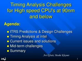
Timing Analysis Challenges for High speed CPU's at 90nm and below. ITRS Predictions & Design Challenges Timing Analysis at intel Current issues and solutions Mid-term challenges Summary. Agenda:. Avi Efrati, Moshe Kleyner. The VLSI Chip in 2010. Process Technology. 25nm gate length.

E N D
Timing Analysis Challenges for High speed CPU's at 90nm and below • ITRS Predictions & Design Challenges • Timing Analysis at intel • Current issues and solutions • Mid-term challenges • Summary Agenda: Avi Efrati, Moshe Kleyner
The VLSI Chip in 2010... Process Technology 25nm gate length Transistors 1,546 M Logic Transistors 300 M 2 Size 280 mm Clock frequency 11.5 GHz Chip I/O’s 3,840 Wiring levels (metals) 9 - 10 Voltage 0.8 - 1.0 Power 120-218 Watts Supply current ~ 160 Amps Source: ITRS ‘01 roadmap
Timing verification for Intel CPUs • Synchronous design style, mostly • Multiple synchronized clocks, GHz range • NO trend to asynchronous design in near future • Deep pipelining • Internal static timer – Tango • Cell-based, using abstract models for custom blocks • Handles transparent latches and sequential transparent loops, both BFS and DFS timing propagation options • Generates and uses proprietary abstract timing model for hierarchical timing • At each level an abstract timing model can be created for next level • Typically 2-3 timing hierarchy levels • PathMill used at device-level, produces same abstract model
What’s under the hood ? • Handling transparent loops • False paths • Hierarchical Analysis • Shell models
Loops… clk clk# • Combinational loops are disallowed • Local self-resetting circuitry may exist • Sequential loops exist • Formed by combinational paths and transparent latches • Actually form SCC (Strongly connected component), handled automatically • Typical for FSM implemented with Latches clk clk2
g g c c a a b b z z g d d e e c g g f f g a c c b c z a a d a b g b e z z d b d z c f d e e a e f f b z f d e f c=1 c=0 False Paths • Manual marking of false paths, considered in timing analysis • Automatic SAT-based false paths • Work done with K.Sakallah U.Mich. • Applied in combinational logic b=0 c=1 d=0 e=1 c=0
Hierarchical Analysis • Cannot analyze full-chip at transistor or gate level • Huge data, impractical run-time • Abstract blocks as compact models • Hide internal details not relevant at chip level, assume pre-defined clocks • As accurate as possible electrical interface and timing model • Abstract model supports also timing transparency – BLUE BOX
Electrical Shell elements Core Core MB2 MB1 Flat FC interconnect FF1 FF2 clk clk Q D Q D OUT IN clk clk clk Q Q D D Q D L2 L1 L3 Combinational Cells Shell Model Core • Interface cells and interconnect are preserved • User may select deeper than 1 shell • User may expose some transparent latches • Balance core complexity versus amount of cells exposed in full-chip, Deep Shell Model • Cores are abstract timing models • Full-chip analysis uses shell models of blocks
Current and near-term challenges • CrossTalk impact on timing • Active interconnect • Mixed abstraction, device to full-chip • Use of domino as characterized cells • SoC challenges
CrossTalk impact on Timing • CrossTalk has noise and timing impact • Search for highest peak noise while… • Victim transitions – for timing • Victim stable – for functional noise • CrossTalk timing effect may be approximated as a Miller Xcap multiplier (MCF), but… • Default MCF may over or under-estimate effect • MCF is slope dependent, difficult to set upfront • AWE + superposition gives good results but may be too costly to apply everywhere • Accuracy vs. run-time tradeoff is key • Timing filtering followed by local logic filtering • SMCF (smart MCF) or AWE-based peak • Timing iterations to converge CrossTtalk impact • Very active research in last few years !!
Fitting SMCF to experimental data • Physically MCF depends on L=Tvic/Tagg • Experimentally fitted with equation a-b*exp(-L)
Rcv Drv Rcv “Active” Interconnect • For quite some time interconnect is not negligible, now it becomes active ! • Repeaters may be buffers, inverters, latches, flops • Virtual (early design) or real repeaters • Interconnect may be: • Simple wire • Buffered (inverted or not) • Pipelined (and buffered) • Pipelining the interconnect is considered simultaneously in RTL, Floor Plan and early timing • Mutual Inductance impact being assessed • Asynchronous long-distance on-chip communication ?
Mixed Abstraction • Layout becomes more cell-based…but circuit families in cells are more complex • Some circuits may be characterized as cells, some may require device-level analysis • Fluid cells & device-level optimization • Comprehend devices, cells and abstract models in same run • Single timing graph • May need on-the-fly dynamic analysis on parts of circuit • Use circuit recognition capabilities • Requires stimuli generation • More detailed waves, not only slope • Sophisticated timing checks for domino • Propagate also pulses not only arrival time
Core Mixed-level Timing • Cell, abstracts and devices co-exist at analysis level • Choose flexible abstraction/accuracy trade-off Mixed device/cells/abstracts
Domino characterization • Regular or footless domino as characterized cells • Will be supported in cell-based timing • Additional domino latches, etc… • Delay similar to static cells and latches • Checks are more complex !!…next page keeper clk keeper clk output Domino node Domino node output inputs inputs Domino And2 Footless And2 See Van Campenhout, Sakallah, Mudge paper 1999
Need sufficiently wide pulse at domino node Ensure pulse width to next stage Ensure feedback can hold data Modeling issues Slopes of inputs Pulse width per discharge path Translating inputs intersection into pulse at domino node Dis-allowing min-transparency converts pulse width to setup check Non-transparency hold check precharge eval Domino node a b Domino node Inputs Pulse Width Checks
SoC challenges • Multi-core CPU’s or high-integration SoC • New integration level in all areas – RTL, timing, layout, testing etc… • Timing challenges • New level of hierarchical timing, more need for functionality aware timing, better abstract models • Optimize interfaces without core re-design • Integrative approach, zoom-in from abstract to detailed in same environment • Multiple clocks, possibly asynchronous to each other • Inter-module communication, protocols, early spec and accurate verification • More in-die variation, instances of same module may operate at different Vcc/temperature etc…
Mid-term challenges • MIS – Multiple Input Switching • Process and environment variability • Voltage and Temperature • Process variability • Timing challenges due to leakage reduction techniques • Sleep transistors – usage methodology and support in timing
MIS – Multiple Input Switching • More MIS situations as frequency increases • Less stages in clock cycle • Slope steepness increases slower than frequency • Broad range of effects • Single stage well known • Impact across stages more subtle • Load stage may present different effective load due to Miller coupling • Either slow-down or speed-up • Holding side input by real driver versus “ideal voltage” has accuracy impact • Characterization/modeling issues
Vds incremental across top device In series stack Mitigate with legging a a Effectively adds device strengths b b 12.6% pushout Single input switches One gate slow-down/ speed-up 39.7% speedup Single input switches
a b c o c Two gates, Fanout pull-in • c with a or b or both MIS • Miller coupling c,o • Position dependent • No generic model o o2 o2 miller coupling, droop causes speedup on o single input switching o 15.6% speedup mitigate with legging, pushing down stack if only one signal critical
a b c o/c c/o Fanout Signal Location • c with a, b or both MIS • Either speedup or pushout based on connection • connected to pin a: -15.6% to 12.6% variation • connected to pin b: -0.8% to 0.3% variation o o2
MIS – Modeling issues • Not so easy to model in CBD (Cell-Based Design) • Min/Max timing window provides a range of switching times • Window overlap of two inputs allows MIS but doesn’t guarantee it • Assuming full MIS leads to over-design • Most important to check MIS effect on min-delay which may lead to chip failure • Max delay MIS may only reduce operating frequency • Possibly consider max-delay MIS as random variable over overlap window • Easier to consider MIS in BFS timing propagation
Process and Environment Variability • Both deterministic and random variation • The absolute of CD does not decrease at same pace as channel length • Thus relative value of L and Vt variation increases • Lower voltages, higher currents • Non-uniform Vdd on chip, consider Vdd in timing • Big drivers may “starve” neighbors • Are variations causing significant critical path re-ordering ? • “Nominal” timing is not good enough to accurately predict silicon • Worst-casing all effects reduces design space or makes design impossible • Consider chip map for deterministic variations • Need statistical approach in STA for random effects
Reducing leakage power • Most important for mobile and internet servers, as important as speed ! • Standby leakage • power consumed when whole chip is idle, Tj is NOT high (Spec temp. for mobile at 50C) • impact on battery life for portable devices • Active leakage • power consumed due to device leakage when chip is working, and Tj is high (110C) • Subthreshold and Gate leakage significantly higher • impact on overall chip thermal design power and frequency • Ptot=Pswitch + Pleak,,
Block D Block A Block C Block B Sleep Control Sleep Control Sleep Control Sleep Control Leakage Gating with Sleep Transistor • Leakage is a main concern below 90nm • Partition the chip to allow individual control of the sleep transistors • Sleep transistor is on while the block is working • Sleep transistor is off while the block is idle
Sleep transistors in timing • Difficult to comprehend in STA • Many cells share same virtual ground through one sleep transistor (legged/distributed in reality) • Voltage of virtual ground depends on current drawn by all active gates on same sleep transistor • Need to guarantee max/min voltage on virtual ground • How to verify statically min/max GND voltage • Need cell models and interaction models for cells on different virtual ground • Logic grouping, by time of common switching • Estimate current needed in worst case • Lack of support in timing tools is main limiting factor for using this technique
Summary • STA is a key component of chip design • New VDSM and high frequency challenges • Hierarchical models cope with full chip complexity • Electrical interaction across logical hierarchy boundaries • CrossTalk, MIS, variability and more phenomena need efficient solutions • Will require more dynamic device-level analysis within static timing tools • Closer interaction with Logic/Satisfiability
Noel Menezes Florentin Dartu Ken Stevens Vladi Tsipenyuk Uri First Igor Keller Abhijit Dharchoudhury Contributors