Timing Analysis in High-Performance Integrated Circuits: A Comprehensive Overview
This project examines the critical role of timing analysis in designing high-performance integrated circuits, focusing on the challenges and methodologies used to ensure optimal clock frequency performance. We discuss primitive device delay models, types of timing errors (hold time and setup time violations), and the differences between area-optimized and delay-optimized approaches. We also explore tools for timing analysis, including QuickSim and Leonardo, along with design flow procedures and their implications for post-layout timing analysis. The findings provide insights for efficient design practices.


Timing Analysis in High-Performance Integrated Circuits: A Comprehensive Overview
E N D
Presentation Transcript
Timing Analysis Chaitanya Bandi Instructor: Dr. Vishwani D. Agrawal ELEC 7770 Advanced VLSI Design Team Project
Need for Timing Analysis • High-performance integrated circuits have traditionally been characterized by the clock frequency at which they operate. • While timing measurements can theoretically be performed using a rigorous circuit simulation, such an approach is liable to be too slow to be practical.
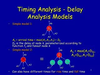
Primitive device delay models • A primitive logic gate has an intrinsic delay.
Methods of Timing Analysis • Static Timing analysis after Synthesis (Pre-Layout Analysis) • Static Timing analysis after Place and Route (also called as Post-Layout Analysis)
Static Timing Analysis Only two kinds of timing errors are possible in such a system: • A hold time violation, when a signal arrives too early, and advances one clock cycle before it should. • A setup time violation, when a signal arrives too late, and misses the time when it should advance.
Area Optimized Vs Delay Optimized From the Synthesis report of the Area and Delay Optimized versions, the Area Optimized version has lesser Area and Delay compared to the Delay Optimized version.
Tools to perform Timing Analysis • QuickSim • Mach TA • Eldo • Leonardo (Results from the Synthesis)
Procedure • Extract the schematic from the Netlist. • Export it as a Spice format. • Force vectors to observe the critical path from the simulation results files. • Find the critical path from the Waveform Viewer (EZWAVE)
Leonardo • The Delays from the Area Optimized netlist shows that the CPU design has a critical path that has a delay of 13.13ns • This is just an estimate of the pre-layout timing analysis. This delay may differ based on the level of optimization.
Further Work • The Post layout incorporates both the block and routing delays as a final analysis of the design’s timing constraints. • Post layout simulation is a better parameter to find the maximum operational frequency and behavior of the circuit.
Suggestions • Technology that is supported by the timing analysers. • 32-bit Processor requires simulation of few days to perform the timing and power analysis. A 16-bit processor would have been a better choice.