Timing Analysis
Timing Analysis. Why Timing Analysis?. timing performance of a design design is free of violations. Two Methods:. Static Timing Analysis Method of validating the timing performance of a design by checking all possible paths for timing violations. Dynamic Timing Analysis

Timing Analysis
E N D
Presentation Transcript
Why Timing Analysis? • timing performance of a design • design is free of violations
Two Methods: • Static Timing Analysis Method of validating the timing performance of a design by checking all possible paths for timing violations. • Dynamic Timing Analysis Determines the full behavior of the circuit for a given set of input stimulus vectors
Advantages and Disadvantages • Static Timing Analysis + faster because it is not necessary to simulate the logical operation of the circuit + checks all the possible paths - only check the timing, not the functionality • Dynamic Timing Analysis + can check the timing and the functionality - consumes more run time - dependent on stimulus vectors
When the Timing Analysis is Done? • First - gate-level design (free of timing violations) placement and routing (accurate delay information or detailed parasitic information) • Second - back-annotated the design results in a layout-accurate timing analysis
Static Timing Analysis Inputs: • gate-level netlist (.db, Verilog, VHDL); delay information in SDF format; timing constraints in Synopsys Design Constraints (SDC) format • Verifies the design timing using information provided in the technology library Outputs: • Timing Report • Timing Models
Timing Checks performed: • Setup, hold, recovery, and removal constraints • User-specified data-to-data timing constraints • Clock-gating setup and hold constraints • Minimum period and minimum pulse width for clocks • Design rules (minimum/maximum transition time, capacitance, and fanout) • Bus contention and floating net conditions
Static Timing Analysis (Violation Checks) PrimeTime breaks the design down into a set of timing paths, calculates the signal propagation delay along each path, and checks for violations of timing constraints inside the design and at the input/output interface.
Timing Paths Each path has a startpoint and an endpoint. The startpoint is a place in the design where data is launched by a clock edge. The data is propagated through combinational logic in the path and then captured at the endpoint by another clock edge. The startpoint of a path is a clock pin of a sequential element, or possibly an input port of the design (because the input data can be launched from some external source). The endpoint of a path is a data input pin of a sequential element, or possibly an output port of the design (because the output data can be captured by some external sink).
How many timing paths? Path 1 Path 2 Path 3 Path 4 Path 1 starts at an input port and ends at the data input of a sequential element. Path 2 starts at the clock pin of a sequential element and ends at the data input of a sequential element. Path 3 starts at the clock pin of a sequential element and ends at an output port. Path 4 starts at an input port and ends at an output port.
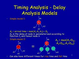
A combinational logic cloud might contain multiple paths. Tool (PrimeTime) uses the longest path to calculate a maximum delay or the shortest path to calculate a minimum delay. • Clock path (a path from a clock input port or cell pin, through one or more buffers or inverters, to the clock pin of a sequential element) for data setup and hold checks • Clock-gating path (a path from an input port to a clock-gating element) for clock-gating setup and hold checks • Asynchronous path (a path from an input port to an asynchronous set or clear pin of a sequential element) for recovery and removal checks • Critical Path (path between an input and an output with the maximum delay) for finding the maximum frequency
Delay Calculation The total delay of a path is the sum of all cell and net delays in the path • Cell Delay Cell delay is the amount of delay from input to output of a logic gate in a path • Net Delay Net delay is the amount of delay from the output of a cell to the input of the next cell in a timing path
Constraint Checking • A setup constraint specifies how much time is necessary for data to be available at the input of a sequential device before the clock edge that captures the data in the device. This constraint enforces a maximum delay on the data path relative to the clock path. • A hold constraint specifies how much time is necessary for data to be stable at the input of a sequential device after the clock edge that captures the data in the device. This constraint enforces a minimum delay on the data path relative to the clock path.
Constraint Checking The amount of time by which a violation is avoided is called the slack. E.g.: for a setup constraint, if a signal must reach a cell input at no later than 8 ns and is determined to arrive at 5 ns, the slack is 3 ns. A slack of 0 means that the constraint is just barely satisfied. A negative slack indicates a timing violation.
PrimeTime assumes that signals are to be propagated through each data path in one clock cycle. Therefore, when PrimeTime performs a setup check, it verifies that the data path delay is small enough so that the data launched from FF1 reaches FF2 within one clock cycle
Setup check: PrimeTime considers the longest possible delay along the data path and the shortest possible delay along the clock path between FF1 and FF2
Hold check: PrimeTime verifies that the data launched from FF1 reaches FF2 no sooner than the capture clock edge for the previous clock cycle. This check ensures that the data already existing at the input of FF2 remains stable long enough after the clock edge that captures data for the previous cycle. PrimeTime considers the shortest possible delay along the data path and the longest possible delay along the clock path between FF1 and FF2. A hold violation can occur if the clock path has a long delay
Timing Exceptions Paths that are not intended to operate or different. • False path – A path that is never sensitized due to the logic configuration, expected data sequence, or operating mode. • Multicycle path – A path designed to take more than one clock cycle from launch to capture. • Minimum/maximum delay path – A path that must meet a delay constraint that you specify explicitly as a time value.
Max Freq = 1/17 = 58.8 Mhz
Timing Models Timing model contains information on the timing characteristics, but not the logical functionality, of a submodule.
Quick timing model - approximate timing model, useful early in the design cycle Extracted model - discards all of the logic of the original netlist and replaces it with a set of timing arcs between clocks, inputs, and outputs Interface logic model - preserves the interface logic of the original netlist and discards the internal register-to-register logic that has already been verified at the module level Stamp model - a timing model defined in a descriptive language, either written manually or translated from a timing description in another form
Advance Features • Multiple clocks and clock frequencies • Automatic false path detection • Transparent latch analysis and time borrowing • Simultaneous minimum/maximum delay analysis for setup and hold constraints • Analysis with on-chip variation of process, voltage, and temperature (PVT) conditions • Case analysis (analysis with constants or specific transitions applied to specified inputs) • Mode analysis (analysis with module-specific operating modes, such as read mode or write mode for a RAM module) • Bottleneck analysis (reporting of cells that cause the most timing violations) • “What-if” analysis without modifying the original netlist, using inserted buffers, resized cells, and modified nets • Analysis of crosstalk effects between physically adjacent nets using the • PrimeTime SI (signal integrity) option
Latest topic in the area of timing analysis • Statistical Static Timing Analysis The statistical models for gate delays are built by examining the delay behavior of the gate at different values of the parameters influenced by process and operating conditions. Process: Fabricated device and interconnect characteristics (variation in the effective gate length, doping concentration, oxide thickness etc Operating conditions: Uncertainty in environmental conditions during the operation of a chip (power supply and temperature fluctuations
The End. Thanks.