Timing Analysis
Timing Analysis. Section 2.4.2. Delay Time. Def: Time required for output signal Y to change due to change in input signal X Up to now, we have assumed this delay time has been 0 seconds. t=0. t=0. Delay Time. In a “real” circuit, it will take tp seconds for Y to change due to X. t=0.

Timing Analysis
E N D
Presentation Transcript
Timing Analysis Section 2.4.2
Delay Time • Def: Time required for output signal Y to change due to change in input signal X • Up to now, we have assumed this delay time has been 0 seconds. t=0 t=0
Delay Time • In a “real” circuit, it will take tp seconds for Y to change due to X t=0 t=tp tp is known as the propagation delay time
Timing Diagram • We use a timing diagram to graphically represent this delay Horizontal axis = time axis Vertical axis = Logical level axis (Logic One or Logic Zero)
Timing Diagram • We see a change in X at t=0 causes a change in Y at t=tp Horizontal axis = time axis Vertical axis = Logical level axis (Logic One or Logic Zero)
Timing Diagram • We also see a change in X at t=T causes another change in Y at t=T+tp We see that logic circuit F causes a delay of tp seconds in the signal
Simple Example – Not Gate Let tp=2 ns Where ns = nanosecond = 1x10⁻⁹ seconds 2ns
Simple Example – 2 Not Gates Let tp=2 ns 4ns 2ns 2ns Total Delay = 2ns + 2ns = 4ns
Simple Example – 2 Not Gates Notes: Time axis is shared among signals Logic levels (1 or 0) are implied, not shown
Simple Example – 2 Not Gates Sometimes dashed vertical lines are added to aid reading diagram 2ns 2ns 2ns 2ns 2ns
Where does this delay come from? Circuit Delay
Circuit Delay • All electrical circuits have intrinsic resistance (R) and capacitance (C). Let’s analyze a simple RC circuit
Circuit Delay – Simple RC Circuit Vin Vout Note:
Circuit Delay – Example Vin Vout Let R=1ohm, C=1F, so that RC=1 second Time Delay is 0.7s or 700 ms for 0.5Vdd Time Delay is 2.3s for 0.9Vdd Time Delay is 4.6s for 0.99 Vdd
Def: tplh tplh = low-to-high propagation delay time This is the time required for the output to rise from 0V to ½ VDD tplh
Def: tphl Tphl = high-to-low propagation delay time This is the time required for the output to fall from Vdd to ½ VDD tphl
Def: tp (propagation delay time) Let’s define tp = propagation delay time as This will be the “average” delay through the circuit
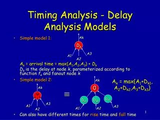
Gate Delay – Simple RC Model Ideal gate with tp=0 delay RC network Tp=tp_not Equivalent model with Gate delay of tp_not Ideal gate with RC network
Gate Delay - Example X 0 25ns 5ns Y tp_not 0 5ns 30ns We indicate tp on the gate
Combinational Logic Delay Longest delay This circuit has multiple delay paths A-Y = 5ns+5ns+5ns=15ns B-Y = 5ns+5ns+5ns+5ns=20ns C-Y = 5ns+5ns+5ns=15ns D-Y = 5ns Shortest delay Longest delay = 20ns Shortest delay = 5ns
Combinational Logic Delay Longest delay We’ll use the longest delay to represent the logic function F. Let’s call it Tcl for time, combinational logic Shortest delay Longest delay = 20ns
Combinational Logic (CL) Cloud Model Tcl=20ns Tcl=20ns
Logic Simulators Used to simulate the output response of a logic circuit.
Logic Simulations • Three primary types • Circuit simulator (e.g. PSPICE) • “Exact” delay for each gate • Most accurate timing analysis • Very slow compared to other types • Functional Simulation (e.g. Quartus ) • Assumes one unit delay for each gate • Very fast compared to other types • Most inaccurate timing analysis • Timing Simulation (e.g. Quartus) • Assumes “average” tp delay for each gate • Not the fastest or slowest timing analysis • Provides “pretty good” timing analysis
Calculate all delay paths through the circuit shown below What is the shortest and longest delay?
Solution: Calculate all delay paths through the circuit shown below This circuit has multiple delay paths A-Y = 5ns+5ns+10ns=20ns B-Y = 2ns+5ns+5ns+10ns=22ns B-Y = 8ns+5ns+10ns=23ns C-Y = 8ns+5ns+10ns=23ns D-Y = 10ns Shortest path=10ns Longest path=23ns
Given the circuit below, find(a) Expression for the logic function(b) Longest delay in original circuit
Solution: Given the circuit below, find(a) Original logic function(b) Longest delay in original circuit Longest Delay = 7ns+7ns = 14ns
Given the circuit below,(a) Using Boolean Algebra, minimize the logic function(b) Longest delay in minimized circuit Delay times are NOT gates= 2ns; AND,OR gates= 5ns NAND, NOR gates= 7ns; XOR gates: 10ns XNOR gates: 12ns
Solution: Given the circuit below, find(a) Minimized logic function(b) Longest delay in minimized circuit Delay times are NOT gates= 2ns; AND,OR gates= 5ns NAND, NOR gates= 7ns; XOR gates: 10ns XNOR gates: 12ns You can show
Solution: Given the circuit below, find(a) Minimized logic function(b) Longest delay in minimized circuit Delay times are NOT gates= 2ns; AND,OR gates= 5ns NAND, NOR gates= 7ns; XOR gates: 10ns XNOR gates: 12ns Longest delay is 7ns
Given the circuit below,(a) Using a Truth Table and a K-map, minimize the logic function
Solution • Do yourself!
D-FF Timing Section 6.3.3
Def: Clock Period and Switching Frequency Tc 0 Tc = cycle period, seconds Switching frequency,
D-FF Timing Parameters time Timing Diagram Tsu= setup time D must be stable (unchanging) tsu seconds before the clock edge Thd = hold time D must be stable thd seconds after the clock edge. Tq = register delay time Q becomes valid tq seconds after the clock edge. 0 If Tsu or Thd are violated, data are NOT stored in D-FF
Maximum Switching Frequency How fast can our circuits operate
Maximum Switching Frequency Model No feedback and thd=0ns W We need to find the minimum time, Tc,min, needed to propagate a signal from input X to node W.
Maximum Switching Frequency Model No feedback and thd=0ns W From the model, we see that the minimum cycle time is Register Setup time
Timing Diagram Maximum Switching Frequency This model assumes tq+tout < tin+tcl+tsu Tc,min
Clock is too fast!!! We have a setup time violation because the clock is too fast!!!
Correcting a Setup Time Violation • Slow down the clock so that However, in most cases, Tc is a system parameter which cannot be changed. Plus, most users want their designs to go faster not slower. 2. Use a pipeline design. Let’s examine this option more closely.
Pipeline Design Let’s break the F Logic into two components, so that F = F1 + F2 and tcl = tcl1 + tcl2