Download
1 / 28
280 likes | 616 Vues
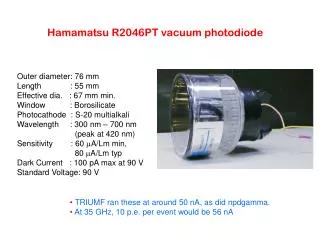
Hamamatsu R2046PT vacuum photodiode. Outer diameter: 76 mm Length : 55 mm Effective dia. : 67 mm min. Window : Borosilicate Photocathode : S-20 multialkali Wavelength : 300 nm – 700 nm (peak at 420 nm)

E N D
Hamamatsu R2046PT vacuum photodiode Outer diameter: 76 mm Length : 55 mm Effective dia. : 67 mm min. Window : Borosilicate Photocathode : S-20 multialkali Wavelength : 300 nm – 700 nm (peak at 420 nm) Sensitivity : 60 mA/Lm min, 80 mA/Lm typ Dark Current : 100 pA max at 90 V Standard Voltage: 90 V • TRIUMF ran these at around 50 nA, as did npdgamma. • At 35 GHz, 10 p.e. per event would be 56 nA
current helicity - + - + - + - 6 A 3.6 pA (0.6 ppm p-p) ( ppm) time Size of Qweak Signal • figure shows regular spin flip; in practice use + - - + or - + + - • for 50 kHz noise bandwidth, rms shot noise is 70 nA • on a scope the noise band would be 100,000 x the signal !
Shot Noise equivalent noise bandwidth [Hz] or [A2] one-sided shot noise, charge quantum [C] current [A]
Integral From Samples (we want the analog bandwidth low) • sample at the center of each interval (n samples) • Q = (sum of samples) x (t) • band limit signal to small fraction of sampling frequency to eliminate the wiggles and kinks. • we impose an analog cutoff at 1/10 the sampling frequency
Averaging of Digitization Noise (we don’t want the analog bandwidth too low) • The 18 bit ADCs have ~0.5 LSB rms noise per sample. • This is reduced by averaging ~500 samples per integration. • This will only work if raw signal spreads over enough channels. • Assuming equivalent noise bandwidth 47 kHz (f3db= 30 kHz) and 18 bit ADC at mid range: • condition Q rms noise before channels channels • (e) integration () (FWHM) • beam ON 50,000 69 mV 1420 3339 • best possible 1 0.31 mV 6.3 15 • So this is OK even for very quiet signals. • Averaging makes integral equivalent to about 21 bits
“noise” = Asymmetry width with 16 ms quartets [4 x (1/250)s] Noise sourceCharge Quantumnoise (ppm) beam-ON shot noise 50,000 e 280 shot noise during LED tests 2,500 e 63 Lowest possible 6.4 mA noise 1 e 1.2 Current source + 1 MW preamp + TRIUMF integrator 2.3 Only cable + 1 MW preamp + integrator 1.4 Comparison of Different Noise Sources for Qweak • Assuming: • 800 MHz event rate • 20 p.e. per event • 2500 PMT gain • 6.4 mA to preamp electronic noise is small compared to counting statistics even the current source test would reach 10-9 (one ppb) in a day
next spin state one spin state – (1/250) second 200 s settling time (not to scale) t 1 ms NIM gate NIM gate Possible DAQ pattern • integrates for 4 ms • stored as four 1 ms integrals • Tsettle as short as 50 s allowed Rapid spin flip reduces noise from target boiling.
Existing Ion Source Signals • Integration triggered by MPS • signals derived from 20 MHz crystal clock • Qweak integrator uses this clock as well
Signals from the current mode scanning polarimeter Peak photodiode current about 50 nA into a 150 MW transimpedance preamplifier
equivalent noise bandwidth [Hz] or [A2] one-sided shot noise, charge quantum [C] current [A] Shot Noise Recap Example, 1 ms integration with beam on, assuming 800 MHz: • Q = 50,000 e • I = 6.4 A (800 MHz x 50,000 e) • B = 500 Hz • in = 7.2 nA rms (7.2 mV with a 1 M preamp) Note that in 1 ms, N = 8 x 10⁵ counts. = 1120 ppm, same as 7.2 nA/6.4 A
“noise” = Asymmetry width with 16 ms quartets [4 x (1/250)s] • Assuming: • 35 GHz event rate for one octant • 10 p.e. per event from vacuum photodiode • 56 nA to preamp • preamp noise 2 ( referred to input). • note that at 20 C and 150 MW, Noise sourceCharge Quantumnoise (ppm)† beam-ON shot noise 10 e 42 lowest possible 56 nA noise 1 e 13 cable +150 MW preamp + integrator ~2 † (divide by ~2 for 1/15 second integral) Comparison of Different Noise Sources for Møller (Note that the beam-on shot noise is the same as counting statistics and can only be reduced by increasing the count rate.)
TRIUMF VME integrator component side: solder side:
Other Noise Thoughts for the Møller Measurement • For the whole detector the counting statistics noise is divided by 8 , but I expect the electronic noise is divided by 16. • Dave Mack points out that, for the current monitors, the relevant noise is for whole detector (42 ppm / 8 = 15 ppm for 16 ms quartets). We should be OK from an electronics standpoint. • We might need ~4 ppm normalization from the Lumis to remove target density fluctuations. Assuming several detectors, we are probably still OK here from an electronics standpoint. • For low noise and high speed the detector-to-preamp distance must be kept small. This will be particularly important if we need high-gain preamps.
Main VME registers • Sample Frequency = system clock / (PERIOD_MULT + 40) • 0 ≤ PERIOD_MULT ≤ 255 • Number of Blocks per integral (1,2,3, or 4) • Samples per Block : 1 ≤ SAMPLE_PER_BLOCK ≤ 16383 • Gate to Trigger Delay = 2.5 ms + (sample period x GATE_DELAY) 0 ≤ GATE_DELAY ≤ 255 • Gate Source: 0=internal, 1=external • System Clock Source: 0=internal, 1=external • Internal Gate Frequency = (100 kHz) / (INT_GATE_FREQ) 1 ≤ INT_GATE_FREQ ≤ 65535 • Individual block sums and total sum for each channel • Firmware Revision Date: REV_DATE always shows the release date of the current firmware revision running in the module August, 2008
Short description of VME Integrator • Quasi-differential isolated BNC connectors – 100 kW from BNC outer conductor to ground. • Input range -10 V to +10 V. Input impedance 12 KW. • Eight integrators per single width VME module. • Module clocked by 20 MHz signal from ion source. Sampling rate set as a fraction of the clock. Range 68 ksps to 500 ksps with 20 MHz clock. • Integration time software selectable – set as a fixed number of samples. (e.g. 2000 samples = 4 ms at 500 ksps) • Module gated by external NIM signal (e.g. MPS). Integration starts a selected time (gate-to-trigger delay) after the leading edge of the gate and runs for preset number of samples. • 32 bit overall sum available to the DAQ via VME bus. This sum can be divided into 1,2,3, or 4 sub- blocks (time intervals) as selected through VME. At full scale, the sum fills up in 1/30 s at 500 ksps. • Internal gate and internal 20 MHz clock provided for testing. • 50 kHz, 5-pole anti-aliasing filter • 18 bit ADC, sample rate up to 500 ksps • Buffered output permits reading previous integral during integration. • Crate power 0.5 A at +12 V and 1.0 A at +5 V August, 2008
+ + - - Signal loss at start of spin states • If polarization has not settled by start of integration, some signal is lost • In the case of the above (+ - - +) quartet, more (+) is lost than (-) • For the parity signal itself, this is only a small part of an already small signal and is likely OK • In the case of helicity correlated current or position it may be a problem
Changing gains and offset on the TRIUMF SNS preamp increasegain increasegain • To open the preamp for adjustment, remove the hex nuts from the OUTPUT side and remove the black screws from the INPUT side. • The rotary gain switches are used to select gain of 10k, 100k, 1M, or 10M. Turn the switch counter-clockwise to increase the gain. • The offset is set for 1.0 volts when shipped, but can be changed with the offset adjust pot.
Integral From Samples (trapezoidal rule) • sample at the sides of each interval (n+1 samples) • Q = (average of first and last samples plus sum of others) x (t) • band limit signal to small fraction of sampling frequency to eliminate the wiggles and kinks. • we impose an analog cutoff at 1/10 the sampling frequency
VME Integrator Front End Quasi-differential Full-differential
Location of adjustments on TRIUMF MK2 “lumi”-style preamp: M Chan 1 gain Offset adjust 50 25 1 0.5 Chan 1 IN Out Chan 2 0.5 1 25 50 +5 V DC Chan 2 gain M
Location of adjustments on TRIUMF MK2 “main”-style preamp: M Chan 1 gain Offset adjust 4 2 1 0.5 Chan 1 IN Out Chan 2 0.5 1 2 4 +5 V DC Chan 2 gain M
Input Cables Large input capacitance increases the noise gain of the first stage. For Qweak we should limit the input cable capacitance to ~200 pf, for example 5m of RG-62. Some typical cables: TYPE Z0(ohm) C(pF/M) diameter(mm) RG-58 53 94.4 5.0 RG-62 93 44.3 6.2 RG-63 125 32.8 10.3
Firmware Running Modes • Integration starts at the preset time (set via VME) after the gate. • We have tried three modes: • No conversion until gate received. • Continuous conversion – integration starts at next sample period. • Continuous conversion, but timing is re-synched on each gate. • We noticed, for 4 ms integrals, 500 ksps, and 4 x 1 ms blocks: • Mode 1 – first block in four block integral was low (~25 mV). • Mode 2 – no difference in blocks, but phase of two modules coulddiffer by half a sample period (1 ms at our 500 ksps). • Mode 3 – initially seemed to solve both problems, but with long runs,detected small residual block difference (1.5 mV with500-sample blocks). Neither the block offset or small time offset can affect the asymmetry Nevertheless, it looks like we can eliminate both by using scheme 3with sufficient gate-to-trigger delay.
shot noise: A Possible Møller Configuration 10 p.e. per event 150 M I-V 35 GHz VME digital signal integrator to DAQ 8.4 V 56 nA vacuum photodiode in shielding outside hall