Flip Chip And Underfills
Flip Chip And Underfills. Hemant Parate Vikas Agarwal. ) . What is Flip Chip?.

Flip Chip And Underfills
E N D
Presentation Transcript
Flip Chip And Underfills Hemant Parate Vikas Agarwal
) ) What is Flip Chip? Flip Chip Technology is an advanced from of surface mount technology, in which bare semiconductor chips are turned upside down, and hence called flip chip (i.e active face down), and bonded directly to a Printed circuit Board or Chip Carrier Substrate Top: Flip Chip; Bottom: SMC
Why Flip Chip • To eliminate the expense, unreliability and low productivity of wirebonding • Wirebonding is peripheral and time consuming bond technique whereas flip chip progressed to area array and allow all I/O’s to be connected simultaneously which allow for high I/O counts at larger pitches and reduced die size • Self aligning chip’s bump pattern to corresponding substrate pad • Shortest possible leads, lowest inductance, highest frequency, best noise control, highest density, greater no of I/O’s, smallest device footprint, reduced cost
How They Are Made: Flow Chart Process • Main Steps: • Bumping • Bonding to Substrate • Underfill
Reasons for Using UBM • UBM is to a flip chip bump what a foundation is to a house • The final metal layer of most IC bond pads is aluminum • Aluminum is not a readily solderable surface, neither wettable nor bondable by most solders and get oxidized when expose to air which acts as an insulator • Adhesion Layer: Adhere to Al pad, the chip passivation, & low contact resistance • Barrier Layer: Diffusion barrier during soldering process • Wetting Layer: good wettability of solder material • Oxidation resistant Barrier: prevent oxidation of the surface
Solder Bumps Types of Solder Bump Formation Techniques: • Evaporation • Electroplating • Printing • Stud Bumping • Direct Placement The result of these methods may differ in bump size and spacing ("pitch"), solder components and composition, cost, manufacturing time, equipment required, assembly temperature, and UBM.
Stud Bumping • Creates conductive gold stud bumps on die bond pads • Connects to substrate with adhesive or ultrasonic assembly • No UBM required • Similar to “ball bonding” process used in wire bonding
In ball bonding, the tip of the gold bond wire is melted to form a sphere. The wire bonding tool presses this sphere against the aluminum bond pad, applying mechanical force, heat, and ultrasonic energy to create a metallic connection. The wire bonding tool next extends the gold wire to the connection pad on the board, substrate, or lead frame, and makes a "stitch" bond to that pad, finishing by breaking off the bond wire to begin another cycle. For gold stud bumping, the first ball bond is made as described, but the wire is then broken close above the ball. The resulting gold ball, or "stud bump" remaining on the bond pad provides a permanent, reliable connection through the aluminum oxide to the underlying metal
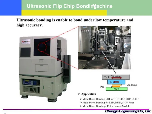
Flip Chip Bonding • Thermocompression • Thermosonic • Adhesives
Thermocompression • Bumps bonded to pads on substrate by force and heat • Process requires gold bumps on the chip and a correspondingly bondable surface (e.g. gold, aluminium) • The bonding temperature is • 300 °C for gold bonding, to soften the material and increase the diffusion bonding process. • Bonding force is 1N for 80um bump
Thermosonic • Ultrasonic energy transferred to the bonding area from the pick-up tool through the back surface of the chip • Main benefit compared to • thermocompression is lower bonding temperature and shorter processing time • Damage may result from from excessive ultrasonic vibrations
Adhesives - isotropic and anisotropic • Ease of processing, low curing temp, elimination of need to clean after the bonding process • Isotropic conductive • adhesives are pastes of epoxy and conducting particle silver that assures conductivity in all direction • Anisotropically conductive adhesives are pastes of thermoplastics filled with metal coated polymer spheres that assures insulation in all direction before bonding and electrically conductivity in z-direction after bonding
Underfill • Non-Conductive adhesive joining surface of chip to substrate. • Protects bumps from moisture or other environmental hazards. • Provides mechanical strength to assembly. • CTE of silicon is 3 ppm/ °C and typical FR4 material is 17 ppm/°C- large strain observed in solder bumps due to this thermal expansion mismatch • Compensates for this mismatch
Underfill Problems • Underfill process is biggest throughput bottleneck in flip chip today. • Dispensing challenges include: • Achieving complete and void-free flow under the die. • Dispensing around closely packed die • Avoiding contamination to other components. • Controlling flux residues.
Testing/Reliability • Testing required at various stages to ensure functionality. • Before solder balls are applied to chip. • After chip is attached to substrate. • After underfill is added and the whole package is complete • Reliability issues with solder ball cracking are tested by cycling the chips through temperature tests from around –50C to 150C.
Advantages • Size • Performance • Flexibility • Reliability • Cost • Widening availability of flip chip materials, equipment, and services
Disadvantages • Lack of standards for procedures due to limited adoption • Manufacturing issues are difficult . . . • Visual verification of bump placement isn’t easy. • Thermal cycle fatigue of solder joints, especially if under fill isn’t used • Viscosity of under fill materials changes with time, therefore wicking process may vary over time of day and shifts • Most ordinary Pb solders have trace quantities of radioactive elements, which may cause soft errors in memory circuits • In fine pitch, solder flux becomes trapped and is very hard to clean. Leading to corrosion effects, gross solder voids, delaminations, etc. • BGA packages present test problems after board mounting with respect to ball integrity. Voids in the joints may lead to reliability issues down the road
Future Market • Worldwide flip chip consumption is over 600,000 units per year. • Projected annual growth of nearly 50% per year.
Emerging Technologies in Flip Chip • Fast-flow, Snap-cure underfill process • Test boards and acoustic imaging of underfill voids. • Flip Chip pin Grid Array Packaging • Fluxless Solder bumping. • Many More in Research • Underfill • Bumping techniques and materials
Test boards and Acoustic Micro imaging A 100 MHz acoustic image shows the condition of the cured underfill.The dark diagonal streaks and corner areas are filler particle aggregation; red features are voids in the underfill in areas of particle aggregation and over the 600 µm diameter uncovered vias near corners. Small open via pattern->
Flip Chip Pin Grid Array Packaging (FCPGA) • Used in Intel Pentium 3 • Pins inserted into a socket. Turned upside down so that the die or the part of the processor that makes up the computer chip is exposed on the top of the processor. By having the die exposed allows the thermal solution to be applied directly to the die, which allows for more efficient cooling of the chip. Figure 1: Pin side view of the FCPGA package
Sources • General trade articles • Electronic Packaging and Production, “Packaging’s Crystall Ball: The 2001 ITRS Roadmap”, Eric Bogatin, 3/1/2002 • SMT Magazine, “Test Boards simplify Flip Chip Underfill Processing”, Karl-Friedrich Becker, March, 2001. • SMT Magazine, “Increased Yield and Reliability of the Flip Chip Process”, Brian J. Lewis, 2002. • Conferences • 2000 Electronics Packaging Technology Conference, IEEE, “Flip Chip Pin Grid Array Packaging Technology”, Hwai Peng Yeoh. • Journal Articles • IEEE Transactions on Advanced Packaging, “Improved Thermal Fatique Reliability for Flip Chip Assemblies Using Redistribution Techniques”, Bart Vandevelde and Eric Beyne, Vol. 23, No.2, May 2000.
Sources cont… • Books • Flip Chip Technologies, ed. John H. Lau, McGraw-Hill, 1996. • Silicon processing for the vlsi era (volume 1-process technology), S.Wolf/R.N. Tauber,Lattice Press, 2000. • Web • www.flipchips.com • www.intel.com • http://extra.ivf.se/ngl/B-Flip-Chip/ChapterB.htm