Download
1 / 14
140 likes | 405 Vues
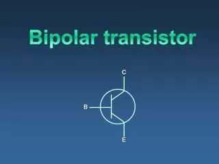
High sensitive bipolar- and high electron mobility transistor read-out electronics for quantum devices. N. Oukhanski and H.-G. Meyer. Contents:. Introduction Bipolar-transistor read-out. PHEMT read-out Motivation Features and construction Measurement setup and procedure

E N D
High sensitive bipolar- and high electron mobility transistor read-out electronics for quantum devices. N. Oukhanski and H.-G. Meyer Contents: Introduction Bipolar-transistor read-out. PHEMT read-out Motivation Features and construction Measurement setup and procedure Results Verification Discussion Summary
Introduction Already known read-out technique for quantum devices. Bipolar-transistor read-out. Easy to match Rsensor with Rnoise of amplifier, TN~80 K.1,2 FET read-out. MinimumTN~2 K @ ~10 kHz, owing RF energy losses.3 SQUID-amplifiers. MinimumTN~1–5 hf/kB. Complex in tuning and setup.4 Pseudomorphic High Electron Mobility Transistor read-out. TN25 K (25 hf/kB)@~20 GHz for ambient temperatures of 1020 K.5, 6, 7 1. N. Oukhanski, V. Schultze, R. P. J. IJsselsteijn, and H.-G. Meyer, Rev. Sci. Instrum. 74, 12, 5189 (2003). 2. N. N. Oukhanski, R. Stolz, V. Zakosarenko, and H.-G. Meyer, Physica C 368, 166 (2002). 3. P. Horowitz and W. Hill, Cambridge Univ. Press, 1989, 2nd ed. v. 2, pp. 53–66. 4. M. Muck, J. B. Kycia, and J. Clarke, Appl. Phys. Lett. 78, 967 (2001). 5. J. Bautista, J. Laskar, P. Szydlik, TDA Progress Report 42-120, 1995. 6. J.E. Fernandez, TMO Progress Report 42-135, pp.1-9, November 15, (1998). 7. I. Angelov, N. Wadefalk, J. Stenarson, E. Kollberg, P. Starski, H. Zirath, IEEE MTT-S, (2000).
Bipolar-transistor read-out. Main features of designed directly-coupled bipolar-transistor electronics Input voltage white noise level is about 0.32nV/Hz1/2. Flicker noise corner frequency as low as 0.1Hz. Current white noise level 6.5pA/Hz1/2. Wide working temperature range: 77-350 K. One-chip FLL unit solution is resistant to ambient condition, i.e. humidity, convection flows, and temperature radiation. Very low thermal drift: 30 nV/K (from 15 to 800C). high symmetrical differential circuits for all parts of the FLL-unit used. full design optimization using simulation with software tool of MicroSim-PSpice. Prototype (left) and integrated version of the FLL unit (right). Gain-bandwidth product fGBP=400 MHz. Three point SQUID biasing possible to reduce voltage drift on the connecting wires to the SQUID. Power consumption: 80 mW at ±1.5 V. Functional diagram of the read-out electronics
Bipolar-transistor read-out. The maximum bandwidth of 6-8 MHz was measured with several types of low-Tc dc-SQUID magnetometers and gradiometers. Maximum slew rate is in the range 3-9M0/s. Minimum measured white flux-noise level with SQUID magnetometer of 1.2-1.70/Hz1/2 (1-1.4fT/Hz1/2). A maximum system dynamic range with the SQUID magnetometer is about 155 dB (50 0). Available with high frequency ac-bias technique with frequency up to 10 MHz.1 Voltage noise spectral density with respect to the input of the integrated electronics at 300 K. Flux and field noise spectrum of SQUID magnetometer with sensitivity B/=0.85 nT/ 0 in three layer shielded can. Maximum system dynamic range in FLL mode 50 0.
PHEMT read-out Already known features. Based on the AlGaAs/InGaAs/GaAs heterostructure. Offers a high transfer coefficient in the microwave frequency range, owing to the high density and mobility of 2DEG along the layer’s heterojunctions (due to an effect of electron space confinement). The unique noise characteristics are derived from the 2DEG’s high electron mobility, which is dependent on the electrons scattering process in heterojunctions. Already measured noise temperatures TN25K (25 hf/kB)@~20 GHz for ambient temperatures of 1020 K. Originally, expected that the HEMTs would be unsuitable for sensitive measurements at frequencies below 100 MHz, because of the high corner frequency of the flicker noise.
Motivation From RF generator USUPP Out Qubit GROOM L C R T=300 K T380 mK UG3 UG1 UG2 Desirable area of application Areas, which need highly sensitive measurements, such as the characterization of qubit circuits,8-11 bolometric measurements,12,13 SQUIDs2 etc., compel us to search for more sensitive readout methods and devices. The principle scheme of resonant circuit readout with PHEMT amplifier. Circuit of interest is inductively coupled to the high-Q parallel resonant circuit, with the directly involved through a short line PHEMT. 8. J.E. Mooij, T.P. Orlando, L. Levitov, Lin Tian, van der Wal, S. Lloyd, Science 285, 1036, (1999). 9. E. Il’ichev, V. Zakosarenko, L. Fritzsch, R. Stolz, H. E. Hoenig, H.-G. Meyer, A.B. Zorin, V.V. Khanin, M. Götz, A.B. Pavolotsky, and J. Niemeyer, Rev. Sci. Instr., 72, 1882, (2001). 10. E. Il’ichev, Wagner Th., Fritzsch L., Kunert J., Schultze V., May T., Hoenig H. E., Meyer H.-G., Grajcar M., Born D., Krech W., Fistul M., Zagoskin A. Appl. Phys. Lett., 80, 4184, (2002). 11. E. Ilґichev, N. Oukhanski, A. Izmalkov, Th. Wagner, M. Grajcar, H.-G. Meyer, A. Yu. Smirnov, Alec Maassen van den Brink, M. H. S. Amin, and A.M. Zagoskin, Phys. Rev. Lett. 91, 9, 097906 (2003). 12. D.-V. Anghel and L. Kuzmin, Appl. Phys. Lett. 88, 293-295 (2003). 13. L. Kuzmin, Proc. Thermal Detector Workshop, Goddard SFC, Washington DC, (2003), to be published.
Features of construction Two amplifier version, based on the commercial PHEMT ATF-35143, have a common layout and were assembled on a printed board of 33x13 mm2 (see Fig. 2). Three-stage construction is used to provide the best conditions for minimizing the input noise temperature and back-action to the tank circuit (in the first stage), maximizing the gain factor (second stage), and impedance matching to the input and output lines (first and third stage). Photo of amplifier To decrease the power consumption and improve low frequency noise performance: We reduced the transistor’s drain voltage to 0.1 V (2 % of Vds) and the drain current to 200 A (0.3 % of Idss). the first stage power dissipation was only 20 W. All resistances in the amplifier’s signal channel were replaced by inductances. To protect the amplifier from external and self interferences we used symmetric design. The amplifier was thermally connected to the helium-3 pot of the commercially available refrigerator, “Heliox 2” by Oxford Instruments with temperature below 400mK.
Measurement setup and procedure 50 Ohm trans. line, K5(f)= 0.042dB loss @ 2.5MHz 50 Ohm divider, K4(f)= -67.113 dB trans. coeff. @ 2.5MHz T380 mK SV RIN 10 k USUPP PHEMT Amplifier, with gain K3(f) Network Analyser HP4396B UG3 50 Ohm trans. line, K1(f)= 0.042dB loss @ 2.5MHz UG1 UG2 Room temperature amplifier with gain K2(f) Out T380 mK PHEMT amplifier L C R Measurements with resistor at T0.38 K To provide a good thermal contact between the source resistor RIN and 3He pot, a copper finger was used. Noise temperature3, 14 SVCOM- input voltage noise spectrum Measurements with resonant circuit Active resistance of resonant circuit at resonant frequency (a) The simplified schemeof the amplifier and setup for the noise temperature measurements with resistor (a) and resonant circuit (b). (b) 14. N. Oukhanski, M. Grajcar, E. Il’ichev, and H.-G. Meyer, Rev. Sci. Instrum. 74, 1145 (2003).
Results 1st amplifier version with resistor Measured minimum TN100 mК@1-4 MHz with 10 k input resistor. For used in this case method3,14 TN MIN(RS=RN)=SV1/2SI1/2/2kB,where RS-real part of input resistance, noise resistanceRN=SV1/2/SI1/2, SI1/2=(4kBRSTN-SV)1/2/RS, estimated minimum noise temperature3 is TN MIN7050 mK5035 hf/kB@30MHz, RN21k With resonant circuit(Q=1510, f0=28.6 MHz, L=66 nH, C=470 pF, RS(f0)18 k) Measured upper limit of noise temperaturein optimistic case (assuming that RS(f0) associated only to dissipation noise of the tank circuit and amplifier) is TN(f0)5525 mK (4018 hf/kB). Comparison of the voltage noise for the 1st version of cryogenic amplifier with that for the standard room temperature design and rated parameters. Measured with resistor TN and calculated current noise SI1/2 of 1st amplifier version. TN MIN(RS=RN) – estimated minimum noise temperature. Inset are the noise of tank circuit, coupled to the input of the 1st (a) and 2d (b) amplifier version.
Results Gate Drain Cgd Rd Cgs Rg Td Tg gmVgs Rds Rgs Rs Source T380 mK USUPP L C R UG1 Back-action noise:15Tba=TN-Tad Additivecomponent Tad (measured without input source),15 originate mainly from drain noise temperature (Td>>TTg),16back-action component Tba under the influence of drain fluctuations on the tank circuit by means of parasitic capacitor Cgs. For 1st amplifier version Tba~15 mK Sv-measured with shorted input voltage noise. Very high sensitivity applications, where a drain current and/or voltage fluctuation can increase the gate temperature, or can decrease the decoherence time of an input signal, impose strong requirements on Tba 2d amplifier version with resonant circuit(Q=2080, f0=26.77 MHz, L=177 nH, C=200 pF, RS(f0)=61.8 kOhm,) Assuming RS(f0) associated only to dissipation noise: TN(f0)7330 mKat ambient temperatureT=370 mK Back-action noise temperature: Tba=TN-Tad~10 mK Simplified small-signal circuit diagram of PHEMT. Variant of the 1st stage with the lowest designed back-action. 15. A. Vinante, M. Bonaldi, M. Cerdonio, P. Falferi, R. Mezzena, G. A. Prodi, and S. Vitale, Classical and Quantum Gravity, 19, Is. 7, p. 1979 (2002). 16. M. W. Pospieszalski IEEE Trans. on Microwave Theory and Techniques, 37, no. 9, pp. 1340-1350 (1991).
Verification L C RS SV G SI Rd L C Rc SV G SI To be convinced in our estimation we used amplifier noise model based on the definition of voltage and current noise, as SV=2kBTNRN and SI=2kBTN/RN.17 Assuming RS(f0) associated only to dissipation noise, noise temperature: TN(f0)=(SVCOM(f0)-4kBTRS)RN/(2kB(RS2+RN2))(SV SI)1/2/(2kB). Suppose the worst case, when RS(f0) associated with dissipation noise of common resistance (Rd and Rc) and contribution of damping cold resistance from amplifier Rc. Hence SI=(SVCOM-SV)/RS-4kBT/Rd. Taking into account: 1.Maximum quality factor, measured between available tank circuits, with both system (Q2040, f027 MHz, C=100 pF and Q3340, f025 MHz, C=100pF correspondingly). 2.Absence of voltage flicker noise in the working frequency range on the ceramic capacitors which we used in our resonant circuits. The pessimistic value for the noise temperature in this case TN(f0)=(SVSI)1/2/(2kB): TN(f0)=110 mK, and170 mKfor the 1st and 2d variant of electronics correspondingly. 17. T. Ryhanen and H. Seppa, J. Low Temp. Phys. 76, 287 (1989).
Discussion • By taking into account tank circuit quality factor Q=2080 (2d variant of amplifier), this setup gives us an opportunity to perform quantum level measurements with periodical signals, even if the coupling coefficient of the thank circuit to the sensor is less than 1. It is necessary to note, that available in real condition tank circuit impedance can be far from optimum value, which can noticeably increase setup noise temperature. Measurements with Qubit, TN270mK, amplifier ambient temperature ~2K • The second version of the amplifier placed at temperature 2 K was successfully employed for different quantum measurements.11, 18, 1 9 • By taking into account system bandwidth f=100 MHz and rating quality factor Q1000@30 MHz estimated available number of cannels 1000 with f100kHz. 18. M. Grajcar, A. Izmalkov, E. Il'ichev, Th. Wagner, N. Oukhanski, U. Huebner, T. May, I. Zhilyaev, H.E. Hoenig, Ya.S. Greenberg, V.I. Shnyrkov, D. Born, W. Krech, H.-G. Meyer, Alec Maassen van den Brink, and M.H.S. Amin, Phys. Rev. B 69, 060501(R) (2004). 19. A. Izmalkov, M. Grajcar, E. Il'ichev, N. Oukhanski, Th. Wagner, H.-G. Meyer, W. Krech, M.H.S. Amin, Alec Maassen van den Brink, A.M. Zagoskin, Europhys. Lett., 65 (6), pp. 844–849 (2004).
Summary Integrated version of direct coupled bipolar-transistor dc SQUID read-out electronics with minimum noise temperature TN=80 K is presented. Very low thermal drift (30 nV/K) of the electronics and the low corner frequency of flicker noise (0.1 Hz) is useful for realization of long-time experiments. Wide working temperature range of read-out electronics (77–350K) provides system reliability at any climatic conditions. High slew rate (up to 9 M0/s) and sensitivity (0.32 nV/Hz1/2), large bandwidth (6 MHz) and system dynamic range at using of long cable between the sensor and electronics (about of 1–2 meters) well suited for high-precision measurements at unshielded conditions.
Summary and acknowledgment Two versions of a cryogenic PHEMT amplifier designed for quantum device readout and tested at an ambient temperature 380 mK. Noise temperature of the 1st amplifier version is below 11050mK (8040hf/kB)@28.6MHz, estimated from the noise of a coupled inputtank circuit with resistance RS(f0)18 kOhm at the resonant frequency. Its minimum input voltage spectral noise density is 200 pV/(Hz)1/2 and the corner frequency of the 1/f noise is close to 300 kHz. For the amplifier with the lowest designed back-action, the noise temperature below 17070 mK (15060 hf/kB)@26.8 MHz was measured when coupled to an input tank circuit with RS(f0)62 kOhm. The amplifiers’ power consumption is in the range of 100–600 W. The second version of the amplifier with ambient temperature 2 K was successfully employed for different quantum measurements. The authors gratefully acknowledge the discussions and help on the different stages of work of H. E. Hoenig, E. Il'ichev, V. Zakosarenko, R. Stolz, M. Grajcar, Th. Wagner, A. Izmalkov, S. Uchaikin and R. Boucher.