

SlideServe
Menu
Préférences
© SlideServe · v2026

Chip design

ina avatar
8 diapositives · 475 Views · Sep 13, 2014

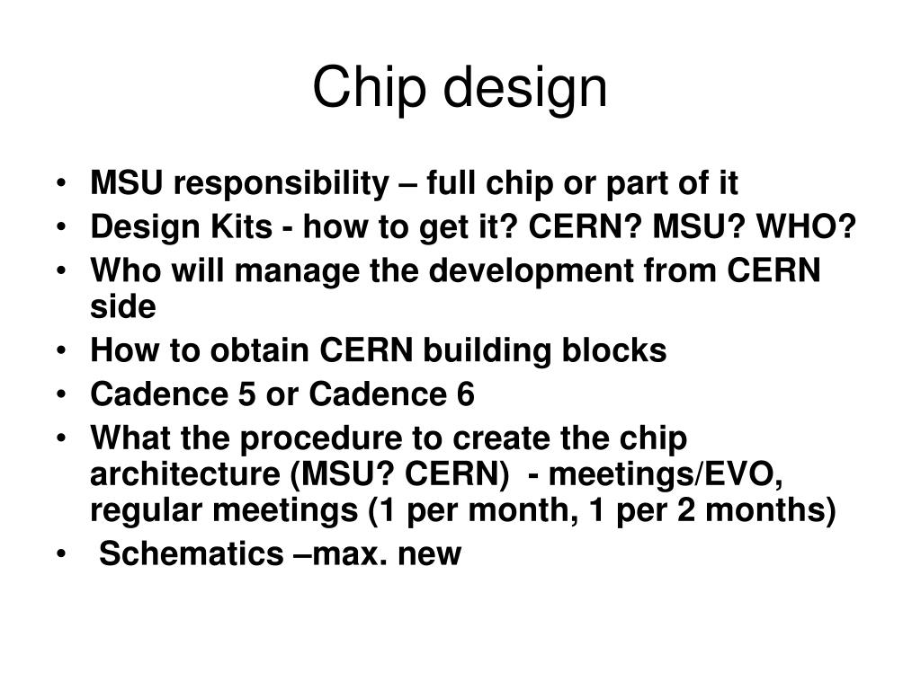
Chip design. MSU responsibility – full chip or part of it Design Kits - how to get it? CERN? MSU? WHO? Who will manage the development from CERN side How to obtain CERN building blocks Cadence 5 or Cadence 6
Chip design - slide 1
01 / 8Chip design
1 / 17

Télécharger la présentation

Chip design
Une image / un lien ci-dessous est fourni (tel quel) pour télécharger la présentation

Politique de téléchargement : le contenu du site vous est fourni TEL QUEL pour votre information et votre usage personnel ; il ne peut être vendu, concédé sous licence ni partagé sur d’autres sites sans l’accord de son auteur.Le contenu vous est fourni TEL QUEL, pour votre information et votre usage personnel uniquement. Téléchargez la présentation en cliquant sur ce lien. Lors du téléchargement, si vous ne parvenez pas à télécharger une présentation, l’éditeur a peut-être supprimé le fichier de son serveur.Pendant le téléchargement, si vous ne parvenez pas à obtenir une présentation, le fichier a peut-être été supprimé par l’éditeur.

F I N

Plus de contenu associé

Transcription de la présentation
  1. Chip design • MSU responsibility – full chip or part of it • Design Kits - how to get it? CERN? MSU? WHO? • Who will manage the development from CERN side • How to obtain CERN building blocks • Cadence 5 or Cadence 6 • What the procedure to create the chip architecture (MSU? CERN) - meetings/EVO, regular meetings (1 per month, 1 per 2 months) • Schematics –max. new

  2. Conception • Conception of Electronics Architecture seems to be realistic • Do we need additional parameters which should been sent to FE (Main things described)? • FE chip should consists of: analog part, ADC, ZS (programmable), Bcnt, config., buffer. Block and interfaces. Synhro 40 MHz. FE Reset, Test pulse, DCnt reset (perhaps something more), transmission data without ZS for testing, min readout delay, no data to out if buffer is full. • Question –why ZS has fluctuation

  3. Conception • Data structure word consists of header band data • Some useful things are in conception as well< we should combine them for the chip specification • Monitoring ZS fluctuation (how) and buffer. • ZS algorithm • Masking noisy and bad channels

  4. Schematics • A lot of questions for some presentation – what is still actual: • SAR ADC • About front-end submicron technologies • ADCN-25 • Protocols • Other chips for LHC

  5. Specification • Sensor thickness • Sensor pitch • Sensor capacitance • MIP level • AC or DC coupling (max dark current) • Single or Double side sensors • Signal/noise, slope • Gain • Dead time • Peaking time

  6. Specification • Linearity • Dynamic range • ADC Bits • Time resolution • Gain stability • Other parameters stability • Radiation hardness • Structure detailed • Power consumption • Supply voltage

  7. Specification • Number of channel • Pedestal parameters (stability) • Connection between chip and detector • Chip geometry • Chip technology • Base line stability • Interfaces • Protection • Load • Out levels

  8. Specification • Pin definition • Occupancy • Time walk • SEU • Adjustment • Description how to work the final structure