4 Bit Arithmetic Logic Unit
4 Bit Arithmetic Logic Unit. Adithya V Kodati Hayagreev Pattabhiraman Vemuri Koneswara Advisor: Dave Parent 12/4/2005. Abstract. Designed a fully functional 4-bit ALU using Philips 74HC/HCT181 schematic. Frequency of operation: 250Mhz Power dissipated : 24.96 mW Area : 676x513uM 2

4 Bit Arithmetic Logic Unit
E N D
Presentation Transcript
4 Bit Arithmetic Logic Unit Adithya V Kodati Hayagreev Pattabhiraman Vemuri Koneswara Advisor: Dave Parent 12/4/2005
Abstract • Designed a fully functional 4-bit ALU using Philips 74HC/HCT181 schematic. • Frequency of operation: 250Mhz • Power dissipated : 24.96 mW • Area : 676x513uM2 • D-flip flops were used to connect the inputs and outputs
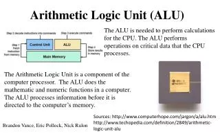
Introduction • The ALU is the basic building block of most digital circuits. Hence having a proper understanding and knowledge of how it should be designed and functions is necessary for a design engineer. • Using CMOS design to implement the functions helps one to understand the design flow as well as adept use of Cadence software. • This project also builds a strong foundation for other advanced design courses which use different processes to implement functionality.
Project Details • Performs full carry look-ahead for arithmetic operation. • 16 arithmetic and 16 logical operations • Works with active high as well as active low inputs • All inputs and outputs are connected via D-flip flops.
Table of functions Courtesy PHILIPS SEMICONDUCTOR
Important lessons learnt • Divide the circuit into cells. Perform DRC and LVS at each stage. • Confine usage of metal3 to the later stages of layout. • Design floor plan and routing of major signals before you start the overall layout. • Use Cadence lab to the maximum extent.
Acknowledgements • Professor Parent • Thanks to Labtam’s Xlitepro for the remote login. • Thanks to Cadence Design Systems for the VLSI lab.