
Datapath and Control
E N D
Presentation Transcript
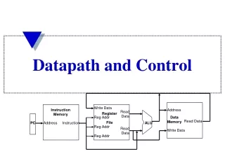
Write Data Instruction Memory Address Read Data Register File Reg Addr Data Memory Read Data PC Address Instruction ALU Reg Addr Read Data Write Data Reg Addr Datapath and Control
Review: Design Principles • Simplicity favors regularity fixed size instructions – 32-bits only three instruction formats • Good design demands good compromises three instruction formats • Smaller is faster limited instruction set limited number of registers in register file limited number of addressing modes • Make the common case fast arithmetic operands from the register file (load-store machine) allow instructions to contain immediate operands
Fetch PC = PC+4 Exec Decode The Processor: Datapath & Control • We're ready to look at an implementation of the MIPS • Simplified to contain only: • memory-reference instructions: lw, sw • arithmetic-logical instructions: add, sub, and, or, slt • control flow instructions: beq, j • Generic implementation (first two stages are same): • use the program counter (PC) to supply the instruction address and fetch the instruction from memory (and update the PC) • decode the instruction (and read registers) • execute the instruction • All instructions (except j) use the ALU after reading the registers
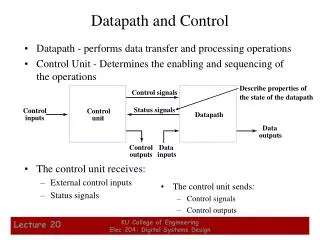
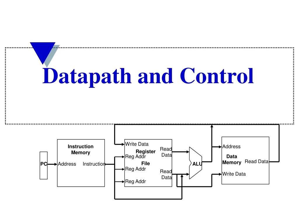
Write Data Instruction Memory Address Read Data Register File Reg Addr Data Memory Read Data PC Address Instruction ALU Reg Addr Read Data Write Data Reg Addr Abstract Implementation View • Two types of functional units: • elements that operate on data values (combinational – like ALU) • elements that contain state (sequential - like registers and memories) • Single cycle operation (multi-cycle presented later) • Split memory (Harvard) model - one memory for instructions and one for data • Does not show how PC is incremented or changed by branch taken, does not show multiplexors or control lines
Address Control Unit Data Memory Read Data Instruction Memory Write Data PC Address Instruction Read Addr 1 Read Data 1 Register File Read Addr 2 ALU Write Addr Read Data 2 overflow Write Data zero Abstract Implementation View
falling (negative) edge cycle time rising (positive) edge Clocking Methodologies • Clocking methodology defines when signals can be read and when they can be written clock rate = 1/(cycle time) e.g., 10 nsec cycle time corresponds to 100 MHz clock rate 1 nsec cycle time corresponds to 1 GHz clock rate • We adopt an edge-triggered clocking methodology • Values stored in the state elements are updated only on a clock edge. Input to combinatorial element are values stored by the state elements in a previous clock cycle, • Combinatorial elements output can be used in the following clock cycle.
State element 1 State element 2 Combinational logic clock one clock cycle Synchronous digital system • All signals must propagate from State element 1 through combinatorial block and to State element 2 in a single clock cycle • The time needed for the logic gates to settle determines the length of the clock cycle. • Assumes state elements are written on every clock cycle; if not, need explicit write control signal - write occurs only when both the write control is asserted and clock edge occurs
Building the Datapath • The datapath assures that data travels between various memory units to registers and ALUs; • The control unit regulates this transfer and determines what actions are to be taken on the data. • It does so using control lines that are connected to various hardware units. • The edge triggered clock methodology allows a given state element to be both read and written in a single clock cycle. • Either we have a long clock cycle for one instruction (length is determined by the slowest instruction), or multiple cycles per instruction.
Add Special ALU that only adds 4 Instruction Memory Instruction Memory is read every cycle, so it doesn’t need an explicit read control signal Read Address PC Instruction PC is updated on every clock cycle Building the Datapath • What are the “building blocks” needed to implement a subset of the MIPS instructions (lw, sw, arithmetic and logic instructions - like add, sub, and, or, slt, and beq)? • Any instruction needs to be fetched and the PC incremented by 4 Extend later for j, beq
Control Unit 5 Read Addr 1 32 5 Read Data 1 Register File Read Addr 2 Instruction 32 Write Addr Read Data 2 Write Data Decoding Instructions • Decoding instructions involves sending the fetched instruction’s opcode and function field bits to the control unit • reading two values from the Register File • Register File addresses are contained in the instruction
31 25 20 15 10 5 0 R-type: op rs rt rd shamt funct ALU control 4 32 Read Addr 1 Read Data 1 Register File Read Addr 2 overflow Instruction zero ALU Write Addr Read Data 2 Write Data The fourth ALU control line supports NOR 32 Executing R Format Operations • R format operations (add, sub, slt, and, or) • perform the indicated (by op and funct) operation on values in rs and rt • store the result back into the Register File (into location rd)
MemWrite 32 Address Data Memory Read Data RegWrite ALU control Write Data 4 32 Read Addr 1 Read Data 1 Register File MemRead Read Addr 2 overflow Instruction zero ALU Write Addr Read Data 2 Write Data 32 Executing R Format Operations • Note that Register File is not written every cycle (e.g. sw), so we need an explicit write control signal for the Register File (RegWrite) • To execute lw or sw operations we need a Data Memory unit with two control signals for write into (MemWrite) and read from (MemRead)
31 25 20 15 0 I-Type: address offset op rs rt Executing Load and Store Operations • Load and store operations compute a memory address by adding the base register (in rs) to the 16-bit signed offset field in the instruction • The 32 bits in the base register were read from the Register File during decode • The offset value in the low order 16 bits of the instruction must be sign extended to create a 32-bit signed value
ALU control RegWrite overflow zero Read Addr 1 Read Data 1 Register File Read Addr 2 Instruction ALU Write Addr MemWrite Read Data 2 Write Data 16-bit offset Address Data Memory Read Data Sign Extend 16 32 Write Data MemRead Executing Load and Store Operations • sw - value read from the Register File during decode must be written to the Data Memory • lw - value read from the Data Memory must be stored in the Register File
31 25 20 15 0 I-Type: address offset op rs rt Executing Branch Operations • Branch operations have to compare the operands read from the Register File during decode (rs and rt values) for equality (zero ALU output is asserted) • compute the branch target address by adding the updated PC to the sign extended 16-bit signed offset field in the instruction • offset value in the low order 16 bits of the instruction must be sign extended to create a 32-bit signed value and then shifted left 2 bits to turn it into a word address
ALU control RegWrite overflow Branch target address Add zero Read Addr 1 Read Data 1 Add 4 Register File Shift left 2 Read Addr 2 Instruction ALU Write Addr Read Data 2 Write Data PC 16 32 16-bit offset Sign Extend Executing Branch Operations PC + 4 (perform a subtraction) (to branch control logic -take branch if zero line is high)
31 25 0 J-Type: op jump target address Add 4 4 Jump address Instruction Memory Shift left 2 28 Read Address PC Instruction 26 Executing Jump Operations • Jump operations have to replace the lower 28 bits of the PC+4 with the lower 26 bits of the fetched instruction shifted left by 2 bits
Creating a Single Datapath from the Parts • We need to assemble the datapath segments, add control lines as needed, and design the control path • Fetch, decode and execute each instruction in one clock cycle – single cycle design. Cycle time is determined by length of the longest path • No datapath resource can be used more than once per instruction, so some must be duplicated (that is why we have a separate Instruction Memory and Data Memory) • To share datapath elements between different instruction classes will need multiplexors at the input of the shared elements • Need control lines to do the selection of inputs
Add MemWrite RegWrite ALU control 4 ovf zero Read Addr 1 Instruction Memory Read Data 1 Address Register File Read Addr 2 Data Memory Read Address PC Instruction Read Data ALU Write Addr R Read Data 2 Write Data Write Data lw / sw R MemRead Sign Extend 16 32 Fetch, R, and Memory Access Portions lw
Add RegWrite ALUSrc ALU control MemWrite MemtoReg 4 ovf zero Read Addr 1 Instruction Memory Read Data 1 Address Register File Read Addr 2 Data Memory Read Address PC Instruction Read Data ALU Write Addr Read Data 2 Write Data Write Data MemRead Sign Extend 16 32 Multiplexor Insertion
Branch not taken, R, lw /sw Add Add 4 Shift left 2 PCSrc RegWrite ALUSrc ALU control MemWrite MemtoReg ovf zero Read Addr 1 Instruction Memory Read Data 1 Address Register File Read Addr 2 Data Memory lw Read Address PC Instruction Read Data R ALU Write Addr Read Data 2 Write Data Write Data R lw / sw MemRead Sign Extend 16 32 Adding the Branch Portion
Datapath - review • We wait for everything to settle down - ALU might not produce “right answer” right away • Cycle time determined by length of the longest path • Split memory (Harvard) model - single cycle operation • Simplified to contain only the instructions: lw, sw, add, sub, and, or, slt, beq. • Sequential components (PC, RegFile, Memory) are edge triggered - state elements are written on every clock cycle; if not, need explicit write control signal • write occurs only when both the write control is asserted and the clock edge occurs
31 25 20 15 10 5 0 R-type: op rs rt rd shamt funct 31 25 20 15 0 I-Type: address offset op rs rt Single cycle datapath • Observations - op field always in bits 31-26 • address of the two registers to be read are always specified by the rs and rt fields (bits 25-21 and 20-16) • address of register to be written is in one of two places – in rt (bits 20-16) for lw; in rd (bits 15-11) for R-type instructions • base register for lw and sw always in rs (bits 25-21) • offset for beq, lw, and sw always in bits 15-0
0 1 PCSrc RegDst RegWrite ALUSrc MemWrite MemtoReg Instr[25-21] Instr[20-16] 0 1 0 1 0 Instr[ 15 -11] 1 MemRead ALU control Instr[5-0] ALUOp (Almost) Complete Single Cycle Datapath Add Add 4 Shift left 2 ovf Read Addr 1 Instruction Memory Read Data 1 Address Register File zero Read Addr 2 Data Memory Read Address PC Instr[31-0] Read Data ALU Write Addr Read Data 2 Write Data Write Data Instr[15-0] Sign Extend 16 32
ALU Control • ALU's operation based on instruction type and function code • MIPS uses multiple control levels to increase speed of the main control unit and decrease its size
ALU control Instr[5-0] ALUOp ALU Control, continued • Multiple levels of control • main control unit generates the ALUOp bits • ALU control unit generates ALU control inputs
ALU Control Truth Table • Can make use of more don’t cares • since ALUOp does not use the encoding 11 • since F5 and F4 are always 10
ALU Control Combinational Logic • From the truth table can design the ALU Control logic
Summary of control lines • RegDest Source of the destination register for the operation • RegWriteEnables writing a register in the register file • ALUsrcSource of second ALU operand, can be a register or part of the instruction • PCsrcSource of the PC (increment [PC + 4] or branch) • MemRead/MemWriteReading / Writing from data memory • MemtoRegSource of write register contents
0 Add Add 1 PCSrc 4 Shift left 2 ALUOp Branch MemRead Control Unit MemtoReg ALUSrc RegWrite MemWrite RegDst ovf Instr[25-21] Read Addr 1 Instruction Memory Read Addr 2 Read Data 1 Address Register File Instr[20-16] zero Data Memory Read Address PC Instr[31-0] 0 Read Data 1 ALU Write Addr Read Data 2 0 1 Write Data 0 Instr[15 -11] Write Data 1 ALU control Instr[15-0] Sign Extend 16 32 Instr[5-0] Datapath with Control Unit Instr[31-26]
R-type lw sw beq RegDst ALUSrc MemtoReg RegWrite MemRead MemWrite Branch ALUOp1 ALUOp0 Control Unit Logic Instr[31] Instr[30] Instr[29] Instr[28] Instr[27] Instr[26] • From the truth table can design the Main Control logic 100011 101011 000100 000000
28 32 Jump 26 Shift left 2 1 Instr[25-0] PC 0 0 1 PCSrc Adding the Jump Operation • J has the opfield 000010 followed by 26-bit jump address. We need to add to the datapath. • The instruction bits [25-0] are shifted left two bits and concatenated to the four MSB of PC+4. PC+4[31-28] • A new multiplexer and control line are needed to select this input for the program counter
R-type lw sw beq RegDst ALUSrc MemtoReg RegWrite MemRead MemWrite Branch ALUOp1 ALUOp0 Control Unit Logic Instr[31] Instr[30] Instr[29] Instr[28] Instr[27] Instr[26] • One more gate is needed in the Main Control logic for J 000010 Jump
Instr[25-0] 1 Shift left 2 28 32 26 0 PC+4[31-28] 0 Add Add 1 4 Shift left 2 PCSrc Jump ALUOp Branch MemRead Instr[31-26] Control Unit MemtoReg MemWrite ALUSrc RegWrite RegDst ovf Instr[25-21] Read Addr 1 Instruction Memory Read Data 1 Address Register File Instr[20-16] zero Read Addr 2 Data Memory Read Address PC Instr[31-0] 0 Read Data 1 ALU Write Addr Read Data 2 0 1 Write Data 0 Instr[15 -11] Write Data 1 Instr[15-0] Sign Extend ALU control 16 32 Instr[5-0] Adding Jump Operation
Control Unit Logic Instr[31] Instr[30] Instr[29] Instr[28] Instr[27] Instr[26] • One more gate is needed in the Main Control logic for Jal 000000 000011 Jal R-type RegDst MemtoReg RegWrite ALUOp1 ALUOp0
Single Cycle Implementation Cycle Time • Unfortunately, though simple, the single cycle approach is not used because it is inefficient • Clock cycle must have the same length for every instruction • What is the longest path (slowest instruction)? • Calculate cycle time assuming negligible delays (for muxes, control unit, sign extend, PC access, shift left 2, wires) except: • Instruction and Data Memory (2ns) • ALU and adders (2ns) • Register File access (reads or writes) (1ns) • floating point operations even longer
What about floating point operations? • A floating point add.d = Instr. Fetch (2 ns)+ Reg. Read (1 ns)+ ALU add(8 ns)+ Reg. Write (1 ns)= 12 ns • Floating point load l.s=2+1+2(ALUop)+2(data mem)+1 (Reg.) = 8 ns • Floating point store s.s =2+1+2(ALU)+2(data mem) = 7 ns. • The longest instruction is floating point multiply mul = Inst. Fetch (2 ns)+Reg. Read (1 ns)+ALU multiply (16 ns)+ Reg. Write (1 ns) = 20 ns • Floating point branch = 5 ns, floating point jump=2 (fetch) • If clock period is variable in length, then we need to look at instruction frequency. For example Loads (31%), stores (21%), R-type (27%), beq(5%), j (2%), add.d, sub.d (7%), mult.d, div.d(7%). • Combining to compute the clock cycle=8x31%+7x21%+6x27%+5x5%+2x2%+20x7%+12x7%= 7 ns
What about variable cycle length? • Instead of a fixed cycle time, we allow cycle time to depend on instruction class. • We can then compare performance, considering that CPI will still be 1, and Instruction count does not change. Perf. CPU variable cycle time = CPU exec. time fixed cycle time Perf. CPU fixed cycle time CPU exec. time var. cycle time = Clock period fixed Clock period variable • because performance= _____________1______________ ) Instr. Count x CPI x Clock Period • Performance improvement = 20 ns (fixed cycle clock period) = 2.86 faster 7 ns (variable cycle clock period)
Where We are Headed • Single cycle/instr. uses the clock cycle inefficiently – the clock cycle must be timed to accommodate the slowest instruction – we cannot make common case fast. • especially problematic for more complex instructions like floating point multiplications • Single cycle/instr. datapath is wasteful of area since some functional units must be duplicated since they can not be “shared” during an instruction execution • e.g., need separate adders to do PC update and branch target address calculations, as well as an ALU to do R-type arithmetic/logic operations and data memory address calculations
IR Address Memory A Read Addr 1 PC Read Data 1 Register File Read Addr 2 Read Data (Instr. or Data) ALUout ALU Write Addr Write Data Read Data 2 B Write Data MDR Where We are Headed • Another approach • use a “smaller” cycle time • have different instructions take different number of cycles • a “multi-cycle” datapath
Multicycle Implementation Overview • Each step in the execution of an instruction takes 1 clock cycle • An instruction takes more than 1 clock cycle to complete • Not every instruction takes thesame number of clock cycles to complete • Multi-cycle implementations allow functional units to be used more than once per instruction as long as they are used on different clock cycles, as a result • we need only one memory • we need only one ALU/adder • We can have faster clock rates
IR Address Memory A Read Addr 1 PC Read Data 1 Register File Read Addr 2 Read Data (Instr. or Data) ALUout ALU Write Addr Write Data Read Data 2 B Write Data MDR The Multicycle Datapath – A High Level View • Registers have to be added after every major functional unit to hold the intermediate output value until that intermediate result is used in a subsequent clock cycle
The Multicycle Datapath – A High Level View • All internal registers hold the intermediate output value until it is used in a subsequent clock cycle of that instruction, thus do not need a dedicated control signal. • The only exception is the Instruction Register (IR), which needs to hold the instruction bits for several cycles, until the instruction finishes its execution. • Thus it needs a control signal which allows it to be written into - IRWrite • Data used by subsequent instructions are stored in programmer visible elements (like Register File, PC or memory)
Multicycle Approach • Break up the instructions into steps where each step takes a cycle while trying to • balance the amount of work to be done in each step • restrict each cycle to use only one major functional unit • Thus each cycle can at most do one of the following operations • a memory access or • a register file access (two reads or one write), or • an ALU operation
System Clock clock cycle IRWrite MemWrite RegWrite IR Address Memory Read Addr 1 A PC Read Data 1 Register File Read Addr 2 Read Data (Instr. or Data) ALUout ALU Write Addr Write Data Read Data 2 B Write Data MDR simplified Clocking the Multicycle Datapath
Multicycle Approach, continued • Reading/writing to any of the internal registers (except IR) or to the PC occurs (quickly) at the end of a clock cycle • reading/writing to the register file takes ~50% of a clock cycle since it has additional control and access overhead (reading can be done in parallel with instruction decode) • All operations occurring in one step occur in parallel within the same clock cycle • This limits us to one ALU operation, one memory access, and one register file access per step (per clock cycle)
IR Address Memory A Read Addr 1 PC Read Data 1 Register File Read Addr 2 Read Data (Instr. or Data) ALUout ALU Write Addr Write Data Read Data 2 B Write Data MDR The Multicycle Datapath – A High Level View • Need more multiplexors to direct the datapath to fewer logical units