Chapter 4 Combinational Logic
This chapter explores the fundamentals of combinational logic circuits used in digital systems. It covers the essential procedures for analyzing logic diagrams and deriving Boolean functions. Step-by-step methods for constructing truth tables from logic diagrams are provided, along with code conversion examples. Additionally, it discusses implementation techniques for various adders, including half-adders, full-adders, and binary adders, emphasizing the challenges of carry propagation and overflow detection in logic circuits. The chapter serves as a resource for understanding the principles of combinational logic in digital design.

Chapter 4 Combinational Logic
E N D
Presentation Transcript
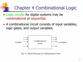
Chapter 4 Combinational Logic • Logic circuits for digital systems may be combinational or sequential. • A combinational circuit consists of input variables, logic gates, and output variables.
4-2. Analysis procedure • To obtain the output Boolean functions from a logic diagram, proceed as follows: • Label all gate outputs that are a function of input variables with arbitrary symbols. Determine the Boolean functions for each gate output. • Label the gates that are a function of input variables and previously labeled gates with other arbitrary symbols. Find the Boolean functions for these gates.
4-2. Analysis procedure • Repeat the process outlined in step 2 until the outputs of the circuit are obtained. • By repeated substitution of previously defined functions, obtain the output Boolean functions in terms of input variables.
Example F2 = AB + AC + BC; T1 = A + B + C; T2 = ABC; T3 = F2’T1; F1 = T3 + T2 F1 = T3 + T2 = F2’T1 + ABC = A’BC’ + A’B’C + AB’C’ + ABC
Derive truth table from logic diagram • We can derive the truth table in Table 4-1 by using the circuit of Fig.4-2.
4-3. Design procedure • Table4-2 is a Code-Conversion example, first, we can list the relation of the BCD and Excess-3 codes in the truth table.
Karnaugh map • For each symbol of the Excess-3 code, we use 1’s to draw the map for simplifying Boolean function.
Circuit implementation z = D’; y = CD + C’D’ = CD + (C + D)’ x = B’C + B’D + BC’D’ = B’(C + D) + B(C + D)’ w = A + BC + BD = A + B(C + D)
4-4. Binary Adder-Subtractor • A combinational circuit that performs the addition of two bits is called a half adder. • The truth table for the half adder is listed below: S = x’y + xy’ C = xy S: Sum C: Carry
Full-Adder • One that performs the addition of three bits(two significant bits and a previous carry) is a full adder.
Simplified Expressions C S = x’y’z + x’yz’ + xy’z’ + xyz C = xy + xz + yz
Another implementation • Full-adder can also implemented with two half adders and one OR gate (Carry Look-Ahead adder). S = z ⊕ (x ⊕ y) = z’(xy’ + x’y) + z(xy’ + x’y)’ = xy’z’ + x’yz’ + xyz + x’y’z C = z(xy’ + x’y) + xy = xy’z + x’yz + xy
Binary adder • This is also called Ripple Carry Adder ,because of the construction with full adders are connected in cascade.
Carry Propagation • Fig.4-9 causes a unstable factor on carry bit, and produces a longest propagation delay. • The signal from Ci to the output carry Ci+1, propagates through an AND and OR gates, so, for an n-bit RCA, there are 2n gate levels for the carry to propagate from input to output.
Carry Propagation • Because the propagation delay will affect the output signals on different time, so the signals are given enough time to get the precise and stable outputs. • The most widely used technique employs the principle of carry look-ahead to improve the speed of the algorithm.
Boolean functions Pi = Ai⊕ Bi steady state value Gi = AiBi steady state value Output sum and carry Si = Pi⊕ Ci Ci+1 = Gi + PiCi Gi : carry generate Pi : carry propagate C0 = input carry C1 = G0 + P0C0 C2 = G1 + P1C1 = G1 + P1G0 + P1P0C0 C3 = G2 + P2C2 = G2 + P2G1 + P2P1G0 + P2P1P0C0 • C3 does not have to wait for C2 and C1 to propagate.
Logic diagram of carry look-ahead generator • C3 is propagated at the same time as C2 and C1.
4-bit adder with carry lookahead • Delay time of n-bit CLAA = XOR + (AND + OR) + XOR
Binary subtractor M = 1subtractor ; M = 0adder
Overflow • It is worth noting Fig.4-13 that binary numbers in the signed-complement system are added and subtracted by the same basic addition and subtraction rules as unsigned numbers. • Overflow is a problem in digital computers because the number of bits that hold the number is finite and a result that contains n+1 bits cannot be accommodated.
Overflow on signed and unsigned • When two unsigned numbers are added, an overflow is detected from the end carry out of the MSB position. • When two signed numbers are added, the sign bit is treated as part of the number and the end carry does not indicate an overflow. • An overflow cann’t occur after an addition if one number is positive and the other is negative. • An overflow may occur if the two numbers added are both positive or both negative.
4-5 Decimal adder BCD adder can’t exceed 9 on each input digit. K is the carry.
Rules of BCD adder • When the binary sum is greater than 1001, we obtain a non-valid BCD representation. • The addition of binary 6(0110) to the binary sum converts it to the correct BCD representation and also produces an output carry as required. • To distinguish them from binary 1000 and 1001, which also have a 1 in position Z8, we specify further that either Z4 or Z2 must have a 1. C = K + Z8Z4 + Z8Z2
Implementation of BCD adder • A decimal parallel adder that adds n decimal digits needs n BCD adder stages. • The output carry from one stage must be connected to the input carry of the next higher-order stage. If =1 0110
4-6. Binary multiplier • Usually there are more bits in the partial products and it is necessary to use full adders to produce the sum of the partial products. And
4-bit by 3-bit binary multiplier • For J multiplier bits and K multiplicand bits we need (J X K) AND gates and (J − 1) K-bit adders to produce a product of J+K bits. • K=4 and J=3, we need 12 AND gates and two 4-bit adders.
4-7. Magnitude comparator • The equality relation of each pair of bits can be expressed logically with an exclusive-NOR function as: A = A3A2A1A0 ; B = B3B2B1B0 xi=AiBi+Ai’Bi’ for i = 0, 1, 2, 3 (A = B) = x3x2x1x0
Magnitude comparator • We inspect the relative magnitudes of pairs of MSB. If equal, we compare the next lower significant pair of digits until a pair of unequal digits is reached. • If the corresponding digit of A is 1 and that of B is 0, we conclude that A>B. (A>B)= A3B’3+x3A2B’2+x3x2A1B’1+x3x2x1A0B’0 (A<B)= A’3B3+x3A’2B2+x3x2A’1B1+x3x2x1A’0B0
4-8. Decoders • The decoder is called n-to-m-line decoder, where m≤2n . • the decoder is also used in conjunction with other code converters such as a BCD-to-seven_segment decoder. • 3-to-8 line decoder: For each possible input combination, there are seven outputs that are equal to 0 and only one that is equal to 1.
Decoder with enable input • Some decoders are constructed with NAND gates, it becomes more economical to generate the decoder minterms in their complemented form. • As indicated by the truth table , only one output can be equal to 0 at any given time, all other outputs are equal to 1.
A B Demultiplexer D0 D1 D2 D3 E Demultiplexer • A decoder with an enable input is referred to as a decoder/demultiplexer. • The truth table of demultiplexer is the same with decoder.
Implementation of a Full Adder with a Decoder • From table 4-4, we obtain the functions for the combinational circuit in sum of minterms: S(x, y, z) = ∑(1, 2, 4, 7) C(x, y, z) = ∑(3, 5, 6, 7)
4-9. Encoders • An encoder is the inverse operation of a decoder. • We can derive the Boolean functions by table 4-7 z = D1 + D3 + D5 + D7 y = D2 + D3 + D6 + D7 x = D4 + D5 + D6 + D7
Priority encoder • If two inputs are active simultaneously, the output produces an undefined combination. We can establish an input priority to ensure that only one input is encoded. • Another ambiguity in the octal-to-binary encoder is that an output with all 0’s is generated when all the inputs are 0; the output is the same as when D0 is equal to 1. • The discrepancy tables on Table 4-7 and Table 4-8 can resolve aforesaid condition by providing one more output to indicate that at least one input is equal to 1.
Priority encoder V=0no valid inputs V=1valid inputs X’s in output columns represent don’t-care conditions X’s in the input columns are useful for representing a truth table in condensed form. Instead of listing all 16 minterms of four variables.
4-input priority encoder • Implementation of table 4-8 x = D2 + D3 y = D3 + D1D’2 V = D0 + D1 + D2 + D3 0 0 0 0
4-10. Multiplexers S = 0, Y = I0Truth Table S Y Y = S’I0 + SI1 S = 1, Y = I1 0 I0 1 I1
Quadruple 2-to-1 Line Multiplexer • Multiplexer circuits can be combined with common selection inputs to provide multiple-bit selection logic. Compare with Fig4-24. I0 Y I1
Boolean function implementation • A more efficient method for implementing a Boolean function of n variables with a multiplexer that has n-1 selection inputs. F(x, y, z) = (1,2,6,7)
4-input function with a multiplexer F(A, B, C, D) = (1, 3, 4, 11, 12, 13, 14, 15)
Three-State Gates • A multiplexer can be constructed with three-state gates.
4-11. HDL for combinational circuits • A module can be described in any one of the following modeling techniques: • Gate-level modeling using instantiation of primitivegates and user-defined modules. • Dataflow modeling using continuous assignment statements with keyword assign. • Behavioral modeling using procedural assignment statements with keyword always.
Gate-level Modeling • A circuit is specified by its logic gates and their interconnection. • Verilog recognizes 12 basic gates as predefined primitives. • The logic values of each gate may be 1, 0, x(unknown), z(high-impedance).
Gate-level description on Verilog code The wire declaration is for internal connections.
Design methodologies There are two basic types of design methodologies: top-down and bottom-up. Top-down: the top-level block is defined and then the sub-blocks necessary to build the top-level block are identified.(Fig.4-9 binary adder) Bottom-up: the building blocks are first identified and then combined to build the top-level block.(Example 4-2 4-bit adder)