Finite-State Control for Multicycle Datapath 11 October 2013
200 likes | 384 Vues
CDA 3101 Fall 2013 Introduction to Computer Organization. Finite-State Control for Multicycle Datapath 11 October 2013. Review – Multicycle Datapath. Each instruction has multiple stages Each stage takes one cycle Instruction fetch

Finite-State Control for Multicycle Datapath 11 October 2013
E N D
Presentation Transcript
CDA 3101 Fall 2013Introduction to Computer Organization Finite-State Control for Multicycle Datapath 11 October 2013
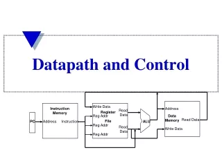
Review – Multicycle Datapath • Each instruction has multiple stages • Each stage takes one cycle • Instruction fetch • Instruction decode / Data fetch • ALU ops / R-format execution • R-format completion • Memory access completion Each stage can re-use hardware from previous stage More efficient use of hardware and time >>New Hardware + Muxes required for buffering, control >>Expanded Control for new hardware All instructions use these
Today: Multicycle DP Control Finite State Control
Basics of Finite State Control (FSC) State: Snapshot of machine (map of ones and zeroes) Transition:Going from one state to another Start State 1 State 0 Requirements for Making Transition Asserted Signals For State 1 Asserted Signals For State 0 Finite State Machine
FSC for Multicycle Datapath High-Level View – Useful for Simplifying Abstractions
FSC for Instr Fetch & Decode Recall: All instr’s. use Instruction/Data Fetch, Decode
Multicycle DP: R-format Step 1: Fetch instr. // Store in IR // Compute PC + 4 Step 2: Decode instruction: opcode, rd, rs, rt, funct fields Data fetch: Apply rs, rt to Register File Data Read into A,B buffer registers (ALUin) Step 3: ALU operation (ALUsrcA, ALUsrcB, ALUop) ALU output goes into ALUout register Step 4: ALUout register contents written to Register File write input Register number in rd written (Assert: RegWrite,RegDst) CPI for R-format = 4 cycles
FSC for R-format Instructions Assume Fetch/Decode completed Set ALU inputs from A,B buffers Perform ALU op per opcode Select Destination Register per rd Write ALUout buffer to Register File Go back for another instruction
Multicycle DP: Store Word (sw) Step 1: Fetch instr. // Store in IR // Compute PC + 4 Step 2: Decode instruction: opcode, rs, rt, offset fields Data fetch: Apply rt to Register File => Base address Data Read into A buffer register (Base) SignExt,Shift offset field into B buffer register Step 3: ALU operation (ALUsrcB, ALUop) => Base + Offset ALU output goes into ALUout register Step 4: ALUout register contents applied as Memory Address Assert: MemWrite [ALUout => RegFile] CPI for Store = 4 cycles
Multicycle DP: Load Word (lw) Step 1: Fetch instr. // Store in IR // Compute PC + 4 Step 2: Decode instruction: opcode, rd, rt, offset fields Data fetch: Apply rt to Register File => Base address Data Read into A buffer register (Base) SignExt,Shift offset field into B buffer register Step 3: ALU operation (ALUsrcB, ALUop) => Base + Offset ALU output goes into ALUout register Step 4: ALUout register contents applied as Memory Address Assert: MemRead Step 5: Memory Data Out routed to Register File write input Register number from rd written to (Assert: CPI for Load = 5 cycles
FSC for Load/Store Instructions Assume Fetch/Decode completed Set ALU inputs from A,B buffers Perform ALU op to get MemAddr Perform Memory Access (read/write) If Load, then do Register Write Go back for another instruction
Multicycle DP: Cond. Branch Step 1: Fetch instr. // Store in IR // Compute PC + 4 Step 2: Decode instruction: opcode, rs, rt, offset fields Data fetch: Apply rs, rt to Register File BTA calc: SignExt,Shift offset field into B buffer register ALU compose PC, offset => BTA Step 3: ALU operation (ALUsrcA, ALUsrcB, ALUop) = compare ALU output present at Zero register causes Control to select BTA or PC+4 CPI for Conditional Branch = 3 cycles
FSC for Branch Instruction Assume Fetch/Decode completed Set ALU inputs from A,B buffers Perform ALU op => BTA Apply BTA or PC+4 to PC Go back for another instruction
Multicycle DP: Jump Step 1: Fetch instr. // Store in IR // Compute PC + 4 Step 2: Decode instruction: opcode, address fields JTA calc: SignExt,Shift offset field [Bits 27-0] Concatenate with PC [Bits 31-28] => JTA Step 3: PC replaced by the Jump Target Address (JTA) PCsource = 10, PCWrite asserted CPI for Jump = 3 cycles
FSC for Jump Instruction Assume Fetch/Decode completed Set PC to be overwritten Hardware composes JTA Apply JTA to PC Go back for another instruction
FSC for Multicycle Datapath 10 states CPI = No. of states encountered on path for that instruction R-format = 4 states Store = 4 states Load = 5 states [0,1,2,3,4] Branch = 3 states Jump = 3 states
Hardware for Multicycle DP FSC Programmable Array Logic (PAL) Register stores State of Finite-State Machine Transition Function
Conclusions • MIPS ISA: Three instruction formats (R,I,J) • One cycle per stage, Different stages per format • One-Cycle StepsR-fmt lw sw beq j • Instruction Fetch • Instruction Decode / Data Fetch • ALU ops / R-format Execution • R-format Completion • Memory Access Completion Finite-State Machine simplifies control design