Experimental set-up and measurements with π and e triggers in HBD
210 likes | 227 Vues
This report details the experimental set-up and measurements conducted with π and e triggers in the HBD detector, including the set-up, measurements, and results.

Experimental set-up and measurements with π and e triggers in HBD
E N D
Presentation Transcript
KEK beam test: report #2 July 7, 2004 • Experimental set-up and trigger • HBD set-up • List of measurements • Results with π trigger • Results with e trigger • HBD as LVL1 trigger
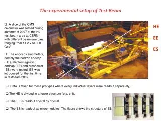
HBD set-up Detector box Radiator box Permanently installed D2 lamp (H120 x V25 x L35 mm) Retractable Fe55 source Stainless steel detector and radiator boxes coupled together. Pumped with turbo molecular pump to unknown vacuum. Total Radiator length (from entrance to mesh): L = 50.2cm Triple GEM 10x10 cm2: GEM1 with CsI layer evaporated on top face. GEM2,3 segmented in four sectors PCB: 9 pads of 3x3 cm2 each (PCB with smaller pads used in last day)
S3 50x45mm S22 10x20mm S1 100x45mm PbGl C2 C1 HBD [947] [845] [15.3] [cm] Experimental Set-up Additional detectors including TPC, CNS-HBD, and an array of Silicon strips detectors • Beam: 1 GeV negative particles (mostly pions with a few percent electrons) • On-line trigger: Coincidence between the three scintillators S1.S22.S3
Part of the real thing Picture taken before installation of S22 in front of HBD
Summary of Measurements (I) • Pedestal runs: • Gain curve with X rays: • Gain monitoring with X rays: 21.05 11:00 Run 10181 VGEM = 495 V ED = +1KV/cm 21.05 201 495 V +1 21.05 202 495 V -0.1 KV/cm 22.05 12:40 268 506 V 22.05 21:50 300 506 V 22.05 10:40 333 506 V 23.05 21:55 355 506 V 24.05 09:30 382 506 or 485 V with the new PCB: 25.05 20:45 517 506V 26.05 08:40 545 506 V 22:15 609 506 V • UV lamp measurements: 12.05 10:30 I on top of GEM1 in vacuum 16-17 pA (p.151) 24.05 IPCB vs ED at VGEM = 442, 474, 506 V data in logbook p. 187- 24.05 I on top of GEM1 vs ED in CF4. Data in logbook p. 189 and p. 191. 24.05 I on top of GEM2 vs ED while amplifying in GEM1 V=506 V Data in p. 190. Set up with the new PCB: 25.05 16:40 I on top of GEM1 in vacuum Data in logbook p. 191. 25.05 17:30 I on top of GEM1 in CF4 191 27.05 00:00 I on top of GEM1 in CF4 199 27.05 08:30 I on top of GEM1 in vacuum 199
Summary of Measurements (II) • First set of measurements (beam was not best aligned and beam intensity low with slits open to ±2 mm). 1 GeV beam S1.S3 trigger VGEM=495V 21.05 20:00 ED = 1 KV/cm Run 10197-199 198K evts 22.05 00:20 ED = - 0.1 KV/cm Runs 10207 – 238 363Kevts • Second set of measurements Beam realigned. New scintillator S2-2 installed in front of HBD. Open slits to ±15 mm. Trigger S1.S3.S2-2. GEMs at 4700 V i.e. VGEM=506V 22.05 14:15 Runs 10271-277 ED =+1KV/cm 100K -0.1 50K -0.2 50K • Third set of measurements (same as the second one but with ED = -0.3 KV/cm) 22/23.05 22:15 Runs 10301 – 335 ED = 1KV/cm 290 Kevts ED = -0.3 KV/cm 360 Kevts • Measurements with new PCB (7 hexagonal pads with a= 7mm) 26.05 09:35 Runs 10548 – 598 ED = +1 KV/cm 164 K -0.1 40 K -0.3 130 K
Summary of Measurements (III) • Three ED scans: 1. VGEM=506V (10Kevts per point) 22.05 19:00 Run 10285 to 10296 ED = +1KV/cm to -0.35 KV/cm 2. VGEM=506V (100Kevts per point) 23.05 10:50 Run 10334 to 10356 ED = +1KV/cm to -0.3 KV/cm 3. VGEM=485V (100Kevts per point) 23.05 21:30 Run 10548 to 10575 ED = +1KV/cm to -0.2 KV/cm
Pion and Electron ID Electron selection cuts: GCC1,2 > 400 & PbGl > 400. Pion selection cuts: GCC1,2 < 300 & 200 < PbGl < 400 & 400 < ToF < 700
Gain variations (I) Pad #5 Assumes: Fe55 x-ray produces 109 e in CF4 dE/dx in CF4 100 e/cm Assumes: Fe55 x-ray produces 109 e in CF4 dE/dx in CF4 126 e/cm
Gain Variations (II) • Electronic gain variations typically less than 5% • Gain variations across the detector up to 20
Positive drift field (I): response to pions Nr. of Events: 310K Pions: 216 244 Pions in HBD: 210 270 ED = +1 KV/cm Single pad response map: Total: 203 720 Using the Fe55 x-rays (109 e) we deduce that the mip signal corresponds to ~19 e
Positive drift field (II): response to electrons ED = +1 KV/cm Mean signal: 288 35 e mip signal * 1.38: 26e Nr. of p.e.: 9 Mean signal: 445 54 e mip signal: 19e Nr. of p.e.: 35 Questions: why there are so many (76%) single pads? where are the expected ~ 40 p.e.?
Negative drift field (I): response to pions ED = -0.3 KV/cm Nr. of Events: 270K Pions: 188 447 Expect in pad #5: 140 393 Pion rejection factor will depend on the threshold that one can safely apply
Negative drift field (II): electron response ED = -0.3 KV/cm Mean signal: 50.8 6 pe Expected signal (ED = -0.3KV/cm): 7 pe
IPE D ED (+) G ET T pA G T ET G I EI Photoelectron Detection Efficiencydetector response vs ED at fixed gain Very efficient detection of photoelectrons even at negative drift fields !!
IPE D ED (+) G ET T pA G T ET G I EI Photoelectron Detection Efficiency remeasured at KEK Results confirmed
pA ED HV(-) CsI relative QE Measure current on mesh resulting from illumination of CsI with UV lamp Current on mesh measured at WI in vacuum: I = 16 pA Current measured at KEK under exactly the same conditions
CF4 Transparency to UV Photons CF4 is transparent
HBD Response Simulation Includes 20 cm absorption length in CF4, lamp shadowing, realistic losses and conservative N0 = 840 cm-1 Total signal 38 e = 29 dE/dx + 9 Cherenkov Blob size: single pad response 78% very similar to data
HBD Response Simulation Normal case, no absorption in CF4, no lamp shadowing, realistic losses and conservative N0 = 840 cm-1 Total signal 62 e = 29 dE/dx + 33 Cherenkov Blob size: single pad 12% more than one pad 88%
HBD as a LVL1 electron trigger Central HIJING event HBD response • Events look clean enough. • HBD could be used to generate • LVL1 electron trigger. • π0 Dalitz and γ conversions produce two • close blobs or an extended blob with double • amplitude. • Algorithm: • Disregard: - two close hits • - single hit with double amplitude • Trigger on isolated blobs • Should provide a powerful trigger for pp, • p(d)A, SiSi, CuCu and at least peripheral • AuAu. Cell threshold: 8fC (5pe) , Cluster threshold: 25fC (16pe)