Download

1 / 22
230 likes | 412 Vues
Explore hybrid h-parameter models for analyzing transistor amplifiers in electronic circuits, with frequency response curves and simplified h-parameter methods.

E N D
Small Signal Analysis Engineered for Tomorrow Manju Khanna Date dd.mm.yy
Subject Name: Electronic Circuits Subject Code: 10CS32 Prepared By: Manju Khanna Department: CSE Date:3/11/2014
Agenda • Small Signal Analysis • Hybrid h-Parameter model for an amplifier • Hybrid Parameters or h-parameters • Transistor Hybrid Model • Analysis of Transistor Amplifier using Complete h- Parameter Model • Analysis of Transistor Amplifier using simplified h-Parameter Model
Small Signal Analysis of Amplifiers • Small signal response is analyzed using the h-parameter model • Response of an amplifier depends on frequency considerations. • Frequency response curves of RC Coupled amplifier , DC amplifier is shown. • There are 3 regions of frequency : low , mid and high • The difference between high and low frequency is the bandwidth
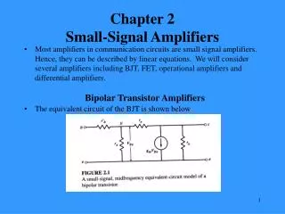
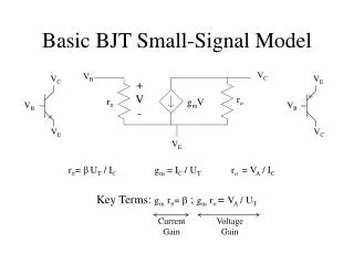
Hybrid h-Parameter model for an amplifier • The equivalent circuit of a transistor can be dram using simple approximation by retaining its essential features. • These equivalent circuits will aid in analyzing transistor circuits easily and rapidly. • A transistor can be treated as a two part network. The terminal behavior of any two part network can be specified by the terminal voltages V1 & V2 at parts 1 & 2 respectively and current i1 and i2, entering parts 1 & 2, respectively, as shown in figure.
Of these four variables V1, V2, i1 and i2, two can be selected as independent variables and the remaining two can be expressed in terms of these independent variables. This leads to various two part parameters out of which the following three are more important.
Hybrid Parameters or h-parameters • If the input current i1 and output Voltage V2 are takes as independent variables, the input voltage V1 and output current i2 can be written as • V1 = h11 i1 + h12 V2 • i2 = h21 i1 + h22 V2 • The four hybrid parameters h11, h12, h21 and h22 are defined as follows. • h11 = [V1 / i1] with V2 = 0 • = Input Impedance with output part short circuited.
h22 = [i2 / V2] with i1 = 0 = Output admittance with input part open circuited. h12 = [V1 / V2] with i1 = 0 = reverse voltage transfer ratio with input part open circuited. h21 = [i2 / i1] with V2 = 0 = Forward current gain with output part short circuited.
The dimensions of h – parameters are as follows: h11 - Ω h22 – mhos h12, h21 – dimension less. as the dimensions are not alike, (i.e) they are hybrid in nature, and these parameters are called as hybrid parameters.
The Hybrid Model for Two-port Network:- V1 = h11 i1 + h12 V2 I2 = h1 i1 + h22 V2 ↓ V1 = h1 i1 + hr V2 I2 = hf i1 + h0 V2
Transistor Hybrid Model • Use of h – parameters to describe a transistor have the following advantages: • h – parameters are real numbers up to radio frequencies . • They are easy to measure • They can be determined from the transistor static characteristics curves. • They are convenient to use in circuit analysis and design. • Easily convert able from one configuration to other. • Readily supplied by manufactories.
Transistor Hybrid Model CE Configuration In common emitter transistor configuration, the input signal is applied between the base and emitter terminals of the transistor and output appears between the collector and emitter terminals. The input voltage (Vbe) and the output current (ic) are given by the following equations: Vbe = hie.ib + hre.Vc ie = hfe.ib + hoe.Vc
Transistor Hybrid Model CB Configuration Where hie =(∂f1/∂iB)Vc = (∂vB/∂iB)Vc = (ΔvB /ΔiB)Vc = (vb / ib)Vc hre =(∂f1/∂vc)IB = (∂vB/∂vc) IB = (ΔvB /Δvc) IB = (vb /vc) IB hfe =(∂f2/∂iB)Vc = (∂ic /∂iB)Vc = (Δ ic /ΔiB)Vc = (ic / ib)Vc hoe= (∂f2/∂vc)IB = (∂ic /∂vc) IB = (Δ ic /Δvc) IB = (ic /vc) IB The same theory is extended to other configurations including CB and CC
Hybrid Model and Equations for the transistor in three different configurations are are given below.
Analysis of Transistor Amplifier using Complete h-Parameter Model In the h-parameter model consider the load Resistance RL and input signal Vs. The expressions for Current gain, Voltage gain ,input and output impedance are: 1. Current Gain: Ai=-hf/(1+hoRL) Where Ai is the current amplification or current gain The overall current gain taking source resistance is given by: Ais=Ai * (Rs/Zi + Rs) where Zi input impedance Rs source resistance
Analysis of Transistor Amplifier using Complete h-Parameter Model 2)Input Impedance(Zi) Zi= hi+hrAiRL 3) Voltage Gain(Av): Av=(Ai * RL)/ Zi Voltage gain taking source resistance is given by Avs=(Av * Zi)/(Zi+Rs) 4) Output Admittance(Yo) Yo=ho-hf * hr/(hi+Rs)
Analysis of Transistor Amplifier using simplified h-Parameter Model Common Emitter Configuration Fixed Bias configuration: Input Impedance Zi = RB || hie Output Impedance Zo=RC || (1/hoe) Voltage gain Av=-hfe * (RC || (1/hoe) /hie Current Gain Ai=hfe * RB/(RB + hie) Voltage Divider Configuration: Input impedance Zi=(RB1 || RB2)|| hie Output Impedance Zo=RC ||(1/hoe) Voltage gain Av=-hfe * [RC || (1/hoe)]/hie Current gain Ai=hfe * (RB1||RB2)/(RB1|| RB2) + hie