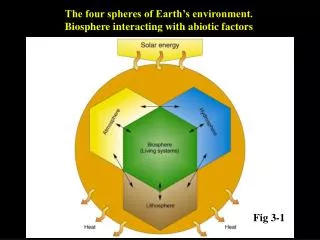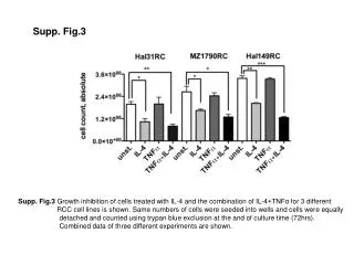
Fig. 3
Towards an Atomic Scale Understanding of Spin Polarized Electron Transport Vincent P. LaBella, College of Nanoscale Science and Engineering, University at Albany / SUNY , DMR 0349108. BEEM. Fig. 1. Magnetic tip. Non-Magnetic tip. azimuthal angle θ. azimuthal angle θ. Fig. 3.
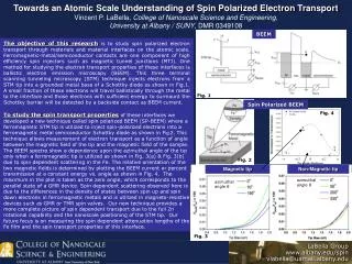

Fig. 3
E N D
Presentation Transcript
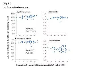
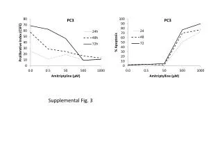
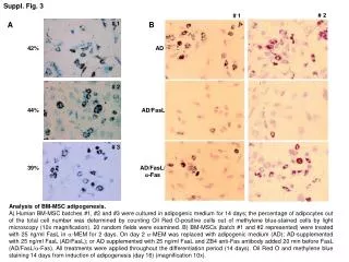
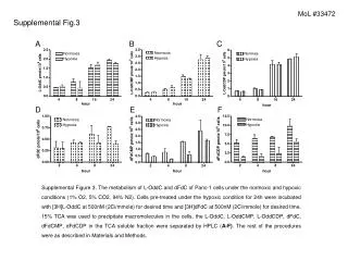
Towards an Atomic Scale Understanding of Spin Polarized Electron TransportVincent P. LaBella, College of Nanoscale Science and Engineering, University at Albany / SUNY, DMR 0349108 BEEM Fig. 1 Magnetic tip Non-Magnetic tip azimuthal angle θ azimuthal angle θ Fig. 3 The objective of this researchis to study spin polarized electron transport through materials and material interfaces on the atomic scale. Ferromagnetic-metal/semiconductor contacts are one component of high efficiency spin injectors such as magnetic tunnel junctions (MTJ). One method for studying the electron transport properties of these interfaces is ballistic electron emission microscopy (BEEM). This three terminal scanning tunneling microscopy (STM) technique injects electrons from a STM tip into a grounded metal base of a Schottky diode as shown in Fig.1. A small fraction of these electrons will travel ballistically through the metal to the interface and those electrons with sufficient energy to surmount the Schottky barrier will be detected by a backside contact as BEEM current. To study the spin transport propertiesof these interfaces we developed a new technique called spin polarized BEEM (SP-BEEM) where a ferromagnetic STM tip is utilized to inject spin-polarized electrons into a ferromagnetic metal semiconductor Schottky diode as shown in Fig.2. This technique allows measurement of electron transport as a function of angle between the magnetic field of the tip and the magnetic field of the sample. The BEEM spectra show a dependence upon the azimuthal angle of the tip only when a ferromagnetic tip is utilized as shown in Fig. 3(a) & Fig. 3(b) due to spin dependent scattering in the Fe. The relative orientation of the two magnetic fields is determined by plotting the BEEM current or percent transmission at a constant energy vs. angle as shown in Fig. 4. The maximum in the plot is taken as the zero angle, which corresponds to the parallel state of a GMR device. Spin dependent scattering observed here is due to the differences in the density of states between spin up and spin down electrons in ferromagnetic metals and is utilized in magneto-resistive devices such as GMR or TMR spin valves. Our new technique provides a more complete picture of spin dependent transport due to the full 2π rotational capability and the nanoscale positioning of the STM tip. Our future focus is on measuring the spin dependent attenuation lengths of the Fe film and the spin transport properties of this interface. Spin Polarized BEEM Fig. 4 Fig. 2
Towards an Atomic Scale Understanding of Spin Polarized Electron TransportVincent P. LaBella, College of Nanoscale Science and Engineering, University at Albany / SUNY, DMR 0349108 PI LaBella tutors sophomore high school student Lexa Vreslovic in quantum mechanics The spintronics research group at CNSE Standing Left to Right: Chaffra Awo-Affoudda, John Garramone, Evan Spadafora, Andy Stollenwerk, Chris Penalver (undergrad)Seated Left to Right: Qa'id Foulks (undergrad), Vincent LaBella (PI) PI LaBella works in the lab with first year grad students and CNSE V.P. Kaloyeros Education and Outreach: The PI is engaged in several educational outreach activities. These include teaching first year graduate students quantum mechanics using an audience response system or clickers. Exposing these first year students to some laboratory research as shown in the top left picture. His research group is composed of a diverse set of students from all over the world that includes 4 Ph.D. students and 2 undergraduates. The PI is also involved in several outreach activities including judging at two high school and middle school science fairs this past spring. In addition, he is tutoring a sophomore high school student in quantum mechanics. The student, Lexa Vreslovic, is engaged in a special topics research program at her high school (The Academy of the Holy Names in Albany NY) where each student picks an interesting topic to study. Lexa picked quantum mechanics after reading an interesting article in Scientific American! This is an ongoing program that Lexa started in her freshman year and plans to continue until she is a senior. Currently she is learning about the double-slit experiment and wave particle duality, next will be tunneling and some hand on experience taking STM images in the laboratory. This study will lead to her competing in local and national level science fairs.