Chapter 17 Feedback, Stability and Oscillators
Chapter 17 Feedback, Stability and Oscillators. Microelectronic Circuit Design Third Edition Richard C. Jaeger and Travis N. Blalock. Chap 17 - 1. Chapter Goals. Review concepts of negative and positive feedback Develop two-port approach to analysis of negative feedback amplifiers

Chapter 17 Feedback, Stability and Oscillators
E N D
Presentation Transcript
Chapter 17Feedback, Stability and Oscillators Microelectronic Circuit Design Third Edition Richard C. Jaeger and Travis N. Blalock Microelectronic Circuit Design, 3E McGraw-Hill Chap 17 - 1
Chapter Goals • Review concepts of negative and positive feedback • Develop two-port approach to analysis of negative feedback amplifiers • Understand topologies and characteristics of series-shunt, shunt-shunt, shunt-series and series-series feedback configurations • Discuss common errors that occur in applying two-port feedback theory • Discuss effects of feedback on frequency response and feedback amplifier stability, and interpret stability in in terms of Nyquist and Bode plots • Apply SPICE ac and transfer function analyses to feedback amplifiers • Determine loop-gain of closed-loop amplifiers using SPICE simulation or measurement • Design operational amplifier frequency compensation using Miller compensation • Develop relationships between op-amp slew rate and unity-gain frequency • Discuss Barkhausen criteria for oscillation and amplitude stabilization • Understand basic RC, LC and crystal oscillator circuits and present LCR model of quartz crystal. Microelectronic Circuit Design, 3E McGraw-Hill Chap 17 - 2
Feedback Effects • Gain Stability: Feedback reduces sensitivity of gain to variations in values of transistor parameters and circuit elements. • Input and Output Impedances: Feedback can increase or decrease input and output resistances of an amplifier. • Bandwidth: Bandwidth of amplifier can be extended using feedback. • Nonlinear Distortion: Feedback reduces effects of nonlinear distortion (e.g. removal of dead zone in class-B amplifiers). Microelectronic Circuit Design, 3E McGraw-Hill Chap 17 - 3
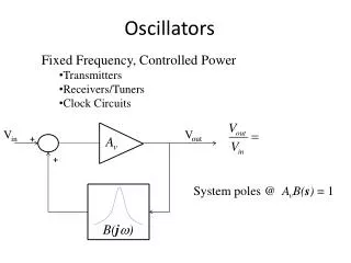
Classic Feedback Systems • A(s) = transfer function of open-loop amplifier or open-loop gain. • b(s) = transfer function of feedback network. • Av(s) = transfer function of closed-loop amplifier or closed-loop gain. T(s) = Ab = loop gain For negative feedback: T(s) > 0 For positive feedback: T(s) < 0 Microelectronic Circuit Design, 3E McGraw-Hill Chap 17 - 4
Classic Feedback Systems Microelectronic Circuit Design, 3E McGraw-Hill Chap 17 - 5
Voltage Amplifiers: Series-Shunt Feedback (Voltage Gain Calculation) Microelectronic Circuit Design, 3E McGraw-Hill Chap 17 - 6
Voltage Amplifiers: Series-Shunt Feedback (Two-Port Representation) • Gain of amplifier should include loading effect of , , RIand RL. • Required h-parameters are found from their individual definitions. • Two-port representation of the amplifier is as shown Microelectronic Circuit Design, 3E McGraw-Hill Chap 17 - 7
Voltage Amplifiers: Series-Shunt Feedback (Input and Output Resistances) Series feedback at a port increases the resistance at that port: Shunt feedback at a port reduces resistance at that port: Microelectronic Circuit Design, 3E McGraw-Hill Chap 17 - 8
Voltage AmplifiersSeries-Shunt Feedback (Example 17.1) • Problem: Find A, b, closed-loop gain, input and output resistances • Given data: R1 = 10 kW, R2 = 91 kW, Rid = 25 kW, Ro = 1 kW, A = 104 • Analysis: Microelectronic Circuit Design, 3E McGraw-Hill Chap 17 - 9
Voltage AmplifiersSeries-Shunt Feedback (Example cont.) Microelectronic Circuit Design, 3E McGraw-Hill Chap 17 - 10
Transresistance Amplifiers: Shunt-Shunt Feedback (Voltage Gain Calculation) Microelectronic Circuit Design, 3E McGraw-Hill Chap 17 - 11
Transresistance Amplifiers: Shunt-Shunt Feedback (Two-Port Representation) • Gain of amplifier should include effects of , , RIand RL. • Required y-parameters are found from their individual definitions. • Two-port representation of the amplifier is as shown. Microelectronic Circuit Design, 3E McGraw-Hill Chap 17 - 12
Transresistance Amplifiers: Shunt-Shunt Feedback (Input and Output Resistances) Resistance at the input port is reduced by shunt feedback: Resistance at the output port is reduced due to shunt feedback: Microelectronic Circuit Design, 3E McGraw-Hill Chap 17 - 13
Transresistance AmplifiersShunt-Shunt Feedback (Example 17.2) • Problem: Find A, b, closed-loop gain, input and output resistances. • Given data: VA = 50 V, bF = 150 • Analysis: For the dc equivalent circuit, Microelectronic Circuit Design, 3E McGraw-Hill Chap 17 - 14
Transresistance AmplifiersShunt-Shunt Feedback (Example cont.) Microelectronic Circuit Design, 3E McGraw-Hill Chap 17 - 15
Current Amplifiers: Shunt-Series Feedback (Voltage Gain Calculation) Microelectronic Circuit Design, 3E McGraw-Hill Chap 17 - 16
Current Amplifiers: Shunt-Series Feedback (Two-Port Representation) • Gain of amplifier should include effects of , , RIand RL. • Required g-parameters are found from their individual definitions. • Two-port representation of the amplifier is as shown Microelectronic Circuit Design, 3E McGraw-Hill Chap 17 - 17
Current Amplifiers: Shunt-Series Feedback (Input and Output Resistances) Shunt feedback at the input port decreases resistance at that port: Series feedback at the output port increases resistance at that port: Microelectronic Circuit Design, 3E McGraw-Hill Chap 17 - 18
Transconductance Amplifiers: Series-Series Feedback (Voltage Gain Calculation) Microelectronic Circuit Design, 3E McGraw-Hill Chap 17 - 19
Transconductance Amplifiers: Series-Series Feedback (Input and Output Resistances) • Gain of amplifier should include effects of , , RIand RL. • Required z-parameters are found from their individual definitions. • Two-port representation of the amplifier is as shown. Series feedback at input and output ports increases resistance at both ports. Microelectronic Circuit Design, 3E McGraw-Hill Chap 17 - 20
Erroneous Application of Two-Port Feedback Theory (Example 17.3) • Problem: Find A, b, closed-loop gain, input and output resistances. • Given data: VREF = 5 V, bo = 100, VA = 50 V, Ao= 10,000, Rid = 25 kW, Ro= 0 • Analysis: The circuit is redrawn to identify the amplifier and feedback networks, and appropriate two-port parameters of the feedback network are found. This case seems to use series-series feedback. ie is sampled by feedback network instead of io. This assumption is made since ao is approximately 1. Microelectronic Circuit Design, 3E McGraw-Hill Chap 17 - 21
Erroneous Application of Two-Port Feedback Theory (cont.) z-parameters are found as shown. From dc equiv.circuit, IE = 1 mA Microelectronic Circuit Design, 3E McGraw-Hill Chap 17 - 22
Erroneous Application of Two-Port Feedback Theory (cont.) Results for Rout are in error because output of op amp is referenced to ground. BJT base current is lost from output port and feedback loop. Rout is limited to 3 and 4 are not valid port terminals as current entering 3 is not same as that exiting 4. Amplifier can’t be reduced to a two-port. SPICE analyses confirm results for Atc and Rin, but results for Rout are in error by a factor of 5000! For Atc and Rin, amplifier can be properly modeled as a series-shunt feedback amplifier, as collector of Q1 can be directly connected to ground for calculations and a valid two-port representation exists as shown. Microelectronic Circuit Design, 3E McGraw-Hill Chap 17 - 23
Analysis of Shunt-Series Feedback Pair (Example 17.4) • Problem: Find A, b, closed-loop gain, input and output resistances. • Given data: bo= 100, VA= 100 V, Q-point for Q1:(0.66 mA, 2.3 V), Q-point for Q2:(1.6 mA, 7.5 V) • Analysis: The circuit is redrawn to identify the amplifier and feedback networks, and appropriate two-port parameters of the feedback network are found. Shunt-shunt transresistance configuration is used. Microelectronic Circuit Design, 3E McGraw-Hill Chap 17 - 24
Analysis of Shunt-Series Feedback Pair (cont.) Small signal parameters are found from given Q-points. For Q1, rp = 3.79 kW, ro = 155 kW. For Q2, rp = 1.56 kW, ro = 64.8 kW. Microelectronic Circuit Design, 3E McGraw-Hill Chap 17 - 25
Analysis of Shunt-Series Feedback Pair (cont.) Closed-loop current gain is given by: The above results are confirmed by SPICE Microelectronic Circuit Design, 3E McGraw-Hill Chap 17 - 26
Analysis of Shunt-Series Feedback Pair (cont.) • If the amplifier is analyzed as a shunt-series configuration, the current gain and input resistance will be calculated correctly, but the output resistance resistance will be in error. Microelectronic Circuit Design, 3E McGraw-Hill Chap 17 - 7
Direct Calculation of Loop Gain Example: is added for proper termination of feedback loop. • Original input source is set to zero. • Test source is inserted at the point where feedback loop is broken. Microelectronic Circuit Design, 3E McGraw-Hill Chap 17 - 28
Calculation of Loop Gain using Successive Voltage and Current Injection Current injection: Current source iX is inserted again at P. Voltage injection: Voltage source vX is inserted at arbitrary point P in circuit. Microelectronic Circuit Design, 3E McGraw-Hill Chap 17 - 29
Simplifications to Successive Voltage and Current Injection Method • Technique is valid even if source resistances with vX and iX are included in analysis. • If at P, RB is zero or RA is infinite, T can be found by only one measurement and T = Tv . In ideal op amp, such point exists at op amp input. • If RA = 0 or RB is infinite, T = TI . • In practice, if RB >> RA or RA >> RB, the simplified expressions can be used. Microelectronic Circuit Design, 3E McGraw-Hill Chap 17 - 30
Blackman’s Theorem • First we select ports where resistance is to be calculated. • Next we select one controlled source in the amplifier’s equivalent circuit and use it to disable the feedback loop and also as reference to find TSC and TOC. RCL = resistance of closed-loop amplifier looking into one of its ports (any terminal pair) RD = resistance looking into same pair of terminals with feedback loop disabled. TSC = Loop gain with a short-circuit applied to selected port TOC = Loop gain with same port open-circuited. Microelectronic Circuit Design, 3E McGraw-Hill Chap 17 - 31
Blackman’s Theorem (Example 17.7) Problem: Find input and output resistances. Given data:VREF = 5 V, R= 5 kW,bo= 100, VA= 50 V, Ao= 10,000, Rid = 25 kW, Ro= 0 Assumptions: Q-point is known, gm= 0.04 S, rp= 25 kW, ro= 25 kW. For output resistance: For input resistance: Microelectronic Circuit Design, 3E McGraw-Hill Chap 17 - 32
Blackman’s Theorem (Example 17.8) Problem: Find input and output resistances. Given data:bo = 100, VA= 100 V, Q-point for Q1:(0.66 mA, 2.3 V), Q-point for Q2:(1.6 mA, 7.5 V). For Q1, rp= 3.79 kW, ro = 155 kW, For Q2, rp = 1.56 kW, ro = 64.8 kW. Microelectronic Circuit Design, 3E McGraw-Hill Chap 17 - 33
Blackman’s Theorem (Example 17.8 cont.) For output resistance: For input resistance: Microelectronic Circuit Design, 3E McGraw-Hill Chap 17 - 34
Blackman’s Theorem (Example 17.9) • Problem: Find expression for output resistance of the Wilson source. Analysis: Feedback loop is disabled by setting reference source i to zero. Assuming gm1= gm2 = gm3 and mf >> bo >> 1. Microelectronic Circuit Design, 3E McGraw-Hill Chap 17 - 35
Use of Feedback to Control Frequency Response Upper and lower cutoff frequencies as well as bandwidth of amplifier are improved, gain is stabilized at where Microelectronic Circuit Design, 3E McGraw-Hill Chap 17 - 36
Use of Nyquist Plot to Determine Stability • If gain of amplifier is greater than or equal to 1 at the frequency where feedback is positive, instability can arise. • Poles are at frequencies where T(s) = -1. • In Nyquist plots, each value of s in s-plane has corresponding value of T(s). • Values of s on jw axis are plotted. • If -1 point is enclosed by boundary, there is some value of s for which T(s) = -1, a pole exists in RHP and the amplifier is unstable. • If -1 point lies outside the interior of the Nyquist plot, all poles of the closed-loop amplifier are in the LHP and the amplifier is stable. Microelectronic Circuit Design, 3E McGraw-Hill Chap 17 - 37
First-Order Systems At dc, T(0) = To, but for w >>1, As w increases, magnitude monotonically approaches zero and phase asymptotically approaches -900. As b changes, value of T(0) = To is scaled. As T(0) changes, radius of circle changes, but it can never enclose the -1 point, so the amplifier is stable regardless of value of To. For a simple low-pass amplifier, It can also represent a single-pole op amp with resistive feedback Microelectronic Circuit Design, 3E McGraw-Hill Chap 17 - 38
Second-Order Systems In given example, T(0) = 14, but for high frequencies As w increases, magnitude monotonically decreases from 14 towards zero and phase asymptotically approaches -180o. The transfer function can never enclose the -1 point, but it can come arbitrarily close to it. Microelectronic Circuit Design, 3E McGraw-Hill Chap 17 - 39
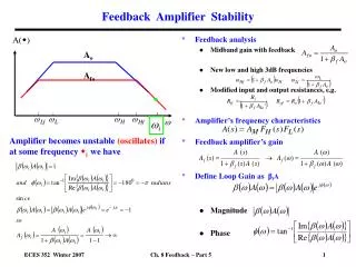
Phase Margin Where First we determine frequency for which magnitude of loop gain is unity, corresponding to intersection of the Nyquist plot with unit circle, and then determine phase shift at this frequency. Difference between this angle and -1800 is phase margin. Small phase margin causes excessive peaking in closed-loop frequency response and ringing in step response. Phase Margin is the maximum increase in phase shift that can be tolerated before the system becomes unstable. Microelectronic Circuit Design, 3E McGraw-Hill Chap 17 - 40
Third-Order Systems For T(0) = 7, but for high frequencies As w increases, the polar plot asymptotically approaches zero along positive imaginary axis. The plot can enclose the -1 point under many circumstances and system is unstable. Microelectronic Circuit Design, 3E McGraw-Hill Chap 17 - 41
Gain Margin where If magnitude of T(jw) is increased by a factor equal to or exceeding gain margin, then closed-loop system becomes unstable, because the Nyquist plot then encloses -1 point. Gain Margin is the reciprocal of magnitude of T(jw) evaluated at frequency for which phase shift is 1800. Microelectronic Circuit Design, 3E McGraw-Hill Chap 17 - 42
Bode Plots - Phase and Gain Margin At 1.2 Mrad/s, magnitude of the loop gain is unity and corresponding phase shift is 145o. Phase margin is given by 180o - 145o = 35o.Amplifier can tolerate additional phase shift of 35o before it becomes unstable. At 3.2 Mrad/s, phase shift is exactly 180o and corresponding magnitude of the loop gain is -17 dB. Phase margin is given by 17 dB.Gain of amplifier must increase by 17 dB before amplifier becomes unstable. Microelectronic Circuit Design, 3E McGraw-Hill Chap 17 - 43
Use of Bode plot to Determine Stability Frequency at which curves corresponding to magnitudes of open-loop gain and reciprocal of feedback factor intersect is the point at which loop gain is unity, phase margin is found from phase plot. Assuming feedback is independent of frequency, For 1/b = 80 dB, fm= 85o, amplifier is stable. For 1/b = 50 dB, fm= 15o, amplifier is stable, but with significant overshoot and ringing in its step response. For 1/b = 0 dB, fm= -45o, amplifier is unstable Microelectronic Circuit Design, 3E McGraw-Hill Chap 17 - 44
Single-pole Op Amp Compensation • Frequency compensation forces overall amplifier to have a single-pole frequency response by connecting compensation capacitor around second gain stage of the basic op amp. Microelectronic Circuit Design, 3E McGraw-Hill Chap 17- 45
Three-stage MOS Op Amp Analysis Input stage is modeled by its Norton equivalent- current source Gmvdm and output resistance Ro. Second stage has gain of gm5ro5= mf5 and follower output stage is a unity-gain buffer. Vo(s) = Vb(s) = - Av2Va(s) For large Av2 Microelectronic Circuit Design, 3E McGraw-Hill Chap 17- 46
Transmission Zeros in FET Op Amps Incorporating the zero determined by gm5 in the analysis, This zero can’t be neglected due to low ratio of transconductances of M2 and M5. Zerocan be canceled by addition of RZ =1/ gm5. Microelectronic Circuit Design, 3E McGraw-Hill Chap 17- 47
Bipolar Amplifier Compensation • Bipolar op amp can be compensated in the same manner as a MOS amplifier • Transmission zero occurs at too high a frequency to affect the response due to higher transconductance of BJT that FET for given operating current. • Unity gain frequency is given by: Microelectronic Circuit Design, 3E McGraw-Hill Chap 17- 48
Slew rate of Op Amp • Slew-rate limiting is caused by limited current available to charge/discharge internal capacitors. For very large Av2, amplifier behaves like an integrator: • For CMOS amplifier, • For bipolar amplifier, Microelectronic Circuit Design, 3E McGraw-Hill Chap 17- 49
Operational Amplifier Compensation (Example 17.10) • Problem: Find value of compensation capacitor for fm = 75o. • Given data:RC1 = 3.3 kW , RC2 = 12 kW ,SPICE parameters: BF = 100, VAF = 75 V, IS = 0.1 fA, RB = 250 W, TF = 0.75 ns, CJC = 2 pF. Assumptions: Dominant pole is set by CC and pnp C-E stage. RZ is included to remove zero associated with CC. pnp and npn transistors are identical; quiescent value of Vo = 0, VJC = 0.75 V, MJC = 0.33. Q4 and Q5 are in parallel, small-signal resistances of diode-connected Q7 and Q8 can be neglected. Microelectronic Circuit Design, 3E McGraw-Hill Chap 17 - 50