Ch 11 Bipolar Transistors and Digital Circuits
310 likes | 1.33k Vues
Ch 11 Bipolar Transistors and Digital Circuits . Examine bipolar junction transistor (BJT) use in inverters for logic circuits. Basic Inverter (RTL) One npn transistor and a load resistor BJT Inverters Transistor-Transistor Logic (TTL) Emitter-Coupled Logic (ECL)

Ch 11 Bipolar Transistors and Digital Circuits
E N D
Presentation Transcript
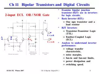
Ch 11 Bipolar Transistors and Digital Circuits • Examine bipolar junction transistor (BJT) use in inverters for logic circuits. • Basic Inverter (RTL) • One npn transistor and a load resistor • BJT Inverters • Transistor-Transistor Logic (TTL) • Emitter-Coupled Logic (ECL) • Analyze to understand inverter performance: • voltage transfer characteristic, • noise margins, • fan-in and fan-out limits, • power dissipation and • switching speed. 2-input ECL OR / NOR Gate Y = A+B A B VR Y = A+B Ch 11 Bipolar Digital Pt. 1
Bipolar Transistor Operation • Transistor regions of operation • Forward Active • VBE > 0 E jnc forward • VBC< 0 C jnc reverse • Cutoff • VBE < 0 E jnc reverse • VBC < 0 C jnc reverse • Saturation • VBE > 0 E jnc forward • VBC > 0 C jnc forward C _ VBC n Collector + + B VCE p Base + _ _ VBE n Emitter E IC Active Ic= βIb Saturation IC< β IB Note: VCE= VBE+VCB = VBE - VBC VCE Cutoff IC ≈ 0 Ch 11 Bipolar Digital Pt. 1
Bipolar Transistor Operation Transistor regions of operation • Forward Active • Electron injection at emitter and collection at collector • VBE > 0 E jnc forward • VBC< 0 C jnc reverse • Ic = β Ib • * Cutoff • * No electron injection at Emitter • VBE < 0 E jnc reverse • VBC < 0 C jnc reverse • IC ≈ 0 • * Saturation • * Electron injection from both E & C • VBE > 0 E jnc forward • VBC > 0 C jnc forward • IC < β IB IC Saturation IC< β IB Active Ic= βIb VCE Cutoff IC≈0 Ch 11 Bipolar Digital Pt. 1
Bipolar Transistor Operation - DC • Base bias VBE determines IB • VCC with RC determine output load line. • Base IB with output load line determines Quiescent Point (VCE , IC ) IC Output Load Line VCE IB VBE IC IB DC Base Current Quiescent Point Base Load Line VCE VBE Ch 11 Bipolar Digital Pt. 1
Bipolar Transistor Operation – Small Signal AC • In small signal amplifiers, • AC signal at input is small –> base current variation is small. • Device moves around DC quiescent point • Device stays in the active region • Amplifier produces current and voltage gain depending upon the configuration, e.g. common emitter (above). iB iC vBE vCE VBB+vi Ch 11 Bipolar Digital Pt. 1
Bipolar Transistor Operation – Digital Circuits • Input signal vi is large. • VBE and IB changes are large. • Important applications digital circuits and power amplifiers • Device can be in active, saturation or cutoff depending on VBE and IB. • Transistor still operates on the load line. • Moves from cutoff thru active to saturation or vice versa as the input signal changes. IC Saturation IC< β IB Active Ic=βIb VCE Cutoff IC≈ 0 Ch 11 Bipolar Digital Pt. 1
Bipolar Transistor Operation - Characteristics • Each region of device operation has its own unique characteristics • Active • Current gain Ic= β Ib • VBE = VBE,active ≈0.7 V (typical value) • VCE,active ≈ ?,NOtypical value! • Saturation • Reduced current gain IC< β IB • VBE = VBE, sat ≈0.8 V(typical value) • VCE = VCE, sat ≈0.2V(typical value) • Cutoff • No current gain IC ≈ 0, IB ≈ 0 • VBE < O • VCE,cutoff ≈ ?,NOtypical value! IC Active Ic= βIb Saturation IC< β IB ~ 0.2 V VCE IB Cutoff IC 0 0.7 V 0.8V VBE Ch 11 Bipolar Digital Pt. 1
Resistor Transistor Logic (RTL) • RTL Logic • Earliest and simplest logic • “0” = low voltage • “1” = high voltage • Inverter is the basic building bock • Combine two inputs in parallel to implement NOR • Combine two inputs in series to implement NAND • Transistors operate in cutoff for low “0”input (base) voltage, so IC ≈ 0 and output is high “1”. • Transistors operate in saturation for high“1” input (base) voltage, so IC ~ mA’s and the output is low “0” due to IR drop across RC. vo vo vi vi Ch 11 Bipolar Digital Pt. 1
Basic Bipolar Transistor Inverter (RTL) • Resistor Transistor Logic (RTL) • For low vi input, output vo is high • Transistor is off (cutoff) since iB ≈ 0 because base-emitter junction is not biased sufficiently (VBE is too small). • Since iB ≈ 0, then iC ≈ 0 because iC ≈βiB. • So vo = VCC - iC RC≈VCC • For high vi input, output vo is low • Transistor is on since iB > 0 because base-emitter junction is biased sufficiently (VBE is large). • Since VBE is large (~0.8 V), iB >> 0, then iC >> 0 since iC ≈βiB. • So vo = VCC - iC RCis very small. • Transistor driven into saturation region so . vo = VCE,sat≈0.2V IB IC n p + n VBE 0.7 V 0.8V VBE IC Active Ic=βIb Saturation IC< β IB VCE ~ 0.2 V Cutoff IC≈ 0 Ch 11 Bipolar Digital Pt. 1
Basic Bipolar Transistor Inverter (RTL) • Transistor operates along load line. • Transistor operates in cutoff when input is low since iB ≈ 0. • As input vi increases, iB increases and transistor moves into active region. • As input vi increases further, transistor moves into saturation region and VCE goes towards zero. + VCE + VBE IC IC Output Load Line active Input high vi large Saturation iC/iB < β Input low vi small 0 cutoff VCE VCE Ch 11 Bipolar Digital Pt. 1
RTL Voltage Transfer Characteristic • Region I (A to B) • Transistor is in cutoff • VBE is small, iB ≈ 0, vo = VCC. • Region II (B to C) • Transistor is on in the active mode (iC = βiB). • iB and VBE are larger; VBE≈ 0.7V • iC andiB increase as vi and VBE increase. • vo and VCE falls as icRC increases. • Region III (C to D) • Transistor is in the saturation mode (iC <βiB). • iB and VBE are larger, VBE≈ 0.8 V • iC is larger • VCE is small, ≈VCE,sat ≈ 0.2V VCC = 5 V IB + VCE + VBE VBE 0.7 0.8 vo A B I II III C D vi Ch 11 Bipolar Digital Pt. 1
Noise Margins • Noise margins are a measure of the reliability of the technology. • Measure of the sensitivity to noise. • Consider one inverter driving an identical inverter. • How large a noise spike can be tolerated before an error occurs? Drive Inverter Load Inverter v01 v02 vi1 vi2 • For output of driver high (v01=VOH), then input of load inverter is high (vi2=VOH ). • A negative noise spike on input of load inverter reduces input signal. • Trouble when net input signal is less than VIH so noise margin is NMH = VOH - VIH . • Similarly, for the low state NML = VIL - VOL . v02 v01 Load Inverter Drive Inverter NML NMH vi1 VOH VOL VIL VIH vi2 Ch 11 Bipolar Digital Pt. 1
RTL Inverter Noise Margins • Noise Margin for Low State • NML = VIL - VOL • VIL = VBE,active= 0.7 V • VOL = VCE,sat = 0.2 V • NML = VIL - VOL = 0.7 V - 0.2 V = 0.5 V • Noise Margin for High State • NMH = VOH - VIH • VOH = VCC = 5 V • VIH= VBE,sat= 0.8 V • NMH = VOH - VIH = 5 V - 0.8 V = 4.2 V • Unequal noise margins for high and low states. VCC = 5 V IB + + VCE VBE VBE 0.7 0.8 vo A B VOH I II III C D NML NMH VOL vi VOH VOL VIL VIH Ch 11 Bipolar Digital Pt. 1
RTL Power Dissipation • Output High State (Low input) • Transistor is in cutoff so iC 0. • No static power dissipation for high state, PH = 0. • Output Low State (High input) • Transistor is in saturation so v o = VCE,sat = 0.2 V. • iC = (VCC - VCE,sat )/RC = (5V - 0.2 V)/10K = 0.48 mA. • PL =VCC iC = (5 V)(0.48 mA) = 2.4 mW • Average P = 1/2(PH + PL) = 1.2 mW VCC = 5 V IB RC = 10K + VCE + VBE VBE 0.7 0.8 vo A B VOH I II III C D VOL vi VIL VIH Ch 11 Bipolar Digital Pt. 1
RTL Propagation Delay • Output going high • Transistor turned off (cutoff) • Charging current flows through RC • tPLH is time it takes the output to rise from VOL = VCE,sat = 0.2 V to 1/2(VOH + VOL) = 2.6 V VCC = 5 V vo iR iCap VCC + vo + C VCE + VBE VCE,sat t tPLH vo A B VOH I II III Long charge – up time! C D VOL vi VIL VIH Ch 11 Bipolar Digital Pt. 1
RTL Propagation Delay • Output going high • Transistor turned off (cutoff) (M N) • Charging current flows through RC • tPLH is time it takes the output to rise from VOL = VCE,sat = 0.2 V to 1/2(VOH + VOL) = 2.6 V (N O) VCC=5V vo iR iCap VCC + vo + C VCE + VCE,sat VBE t Transient Response M N O tPLH vo A B VOH IC I II M III C D P VOL vi N VCE VIL VIH O Ch 11 Bipolar Digital Pt. 1
RTL Propagation Delay • Output going low • Transistor turned on (saturation) and providing discharge current (PR) • But current also flows through RC • tPHL is time it takes the output to fall from VOH = VCC = 5 V to 1/2(VOH + VOL) = 2.6 V(R S) VCC = 5 V vo iR iCap VCC + vo + C + VCE VBE VCE,sat t tPHL vo Transient Response P R S A B VOH IC I II S R III C D VOL P vi VCE VIL VIH Ch 11 Bipolar Digital Pt. 1
RTL Propagation Delay • Output going low VCC = 5 V iR iCap + vo + C + VCE VBE IC S R Short discharge time! P VCE Ch 11 Bipolar Digital Pt. 1
Resistor Transistor Logic (RTL) * RTL provides simple, basic digital technology based on bipolar transistors and resistors. • Logic levels and noise margins • Noise Margin for Low State • NML = VIL – VO = 0.7 V - 0.2 V = 0.5 V • Noise Margin for High State • NMH = VOH - VIH = 5 V - 0.8 V = 4.2 V • Unequal noise margins for high and low states. • Propagation delays • Output going low • Output going high • Propagation delay • Power – Delay Product vo vo vi vi Ch 11 Bipolar Digital Pt. 1