Download

1 / 28
290 likes | 401 Vues
This lecture explores the implementation of Built-In Self-Test (BIST) in VLSI circuits, covering Pattern Generator, LFSR, Response Analyzer, MISR, BIST architectures, and more. Learn about Pseudo-Random Pattern Generation and Matrix Equations for LFSR.

E N D
Lecture 21altBIST -- Built-In Self-Test(Alternative to Lectures 25, 26 and 27) • Definition of BIST • Pattern generator • LFSR • Response analyzer • MISR • Aliasing probability • BIST architectures • Test per scan • Test per clock • Circular self-test • Memory BIST • Summary VLSI Test: Lecture 21alt
Define Built-In Self-Test • Implement the function of automatic test equipment (ATE) on circuit under test (CUT). • Hardware added to CUT: • Pattern generation (PG) • Response analysis (RA) • Test controller CK PG Stored Test Patterns Pin Electronics CUT Test control logic CUT Test control HW/SW BIST Enable RA Stored responses Comparator hardware Go/No-go signature ATE VLSI Test: Lecture 21alt
Pattern Generator (PG) • RAM or ROM with stored deterministic patterns • Counter • Pseudorandom pattern generator • Feedback shift register • Cellular automata VLSI Test: Lecture 21alt
Pseudorandom Integers Xk = Xk-1 + 3 (modulo 8) Xk = Xk-1 + 2 (modulo 8) 0 0 7 1 7 1 Start Start 6 2 6 2 +3 +2 5 3 5 3 4 4 Sequence: 2, 5, 0, 3, 6, 1, 4, 7, 2 . . . Sequence: 2, 4, 6, 0, 2 . . . Maximum length sequence: 3 and 8 are relative primes. VLSI Test: Lecture 21alt
Pseudo-Random Pattern Generation • StandardLinear Feedback Shift Register (LFSR) • Produces patterns algorithmically – repeatable • Has most of desirable random # properties • May not cover all 2n input combinations • Long sequences needed for good fault coverage either hi = 0, i.e., XOR is deleted or hi = Xi Initial state (seed): X0, X1, . . . , Xn-1 must not be 0, 0, . . . , 0 VLSI Test: Lecture 21alt
Matrix Equation for Standard LFSR 0 0 . . . 0 0 1 X0 (t + 1) X1 (t + 1) . . . Xn-3 (t + 1) Xn-2 (t + 1) Xn-1 (t + 1) 0 1 . . . 0 0 h2 … … … … … 0 0 . . . 1 0 hn-2 0 0 . . . 0 1 hn-1 X0 (t) X1 (t) . . . Xn-3 (t) Xn-2 (t) Xn-1 (t) 1 0 . . . 0 0 h1 = X (t + 1) = Ts X (t) (Ts is companion matrix) VLSI Test: Lecture 21alt
LFSR Implements a Galois Field • Galois field (mathematical system): • Multiplication by X same as right shift of LFSR • Addition operator is XOR ( ) • Ts companion matrix: • 1st column 0, except nth element which is always 1 (X0 always feeds back) • Rest of row n – feedback coefficients hi • Remaining identity matrix means a right shift • Near-exhaustive (maximal length) LFSR • Cycles through 2n – 1 states (excluding all-0) VLSI Test: Lecture 21alt
LFSR Properties • Must not initialize to all 0’s – hangs • If X is initial state, LFSR progresses through states X, Ts X, Ts2 X, Ts3 X, … • Matrix period: Smallest k such that Tsk = I • k = LFSR cycle length • Maximum length k = 2n-1, when feedback (characteristic) polynomial is primitive • Example: 1 + X+ X3 • Characteristic polynomial: 1 + h1x + h2X2 + … + hn-1Xn-1 + Xn VLSI Test: Lecture 21alt
D Q X2 D Q X1 LFSR: 1 + X + X3 RESET 100 001 000 010 110 D Q X0 101 111 011 CK RESET X2 X1 X0 Test of primitiveness: Characteristic polynomial of degree n must divide 1 + Xq for q = n, but not for q < n VLSI Test: Lecture 21alt
LFSR as Response Analyzer • Use cyclic redundancy check code (CRCC) generator (LFSR) for response compacter • Treat data bits from circuit POs to be compacted as a decreasing order coefficient polynomial • CRCC divides the PO polynomial by its characteristic polynomial • Leaves remainder of division in LFSR • Must initialize LFSR to seed value (usually 0) before testing • After testing – compare signature in LFSR to precomputed signature of fault-free circuit VLSI Test: Lecture 21alt
Example Modular LFSR Response Analyzer • LFSR seed is “00000” VLSI Test: Lecture 21alt
Signature by Logic Simulation Input bits Initial State 1 0 0 0 1 0 1 0 X0 0 1 0 0 0 1 1 1 1 X1 0 0 1 0 0 0 0 1 0 X2 0 0 0 1 0 0 0 0 1 X3 0 0 0 0 1 0 1 0 1 X4 0 0 0 0 0 1 0 1 0 Signature VLSI Test: Lecture 21alt
Signature by Polynomial Division X5 + X3 + X + 1 Char. polynomial Input bit stream: 0 1 0 1 0 0 0 1 0 ∙ X0 + 1 ∙ X1 + 0 ∙ X2 + 1 ∙ X3 + 0 ∙ X4 + 0 ∙ X5 + 0 ∙ X6 + 1 ∙ X7 X2 X7 X7 + 1 + X5 X5 X5 + X3 + X3 + X3 X3 + X + X + X + X2 + X2 + X2 + 1 +1 remainder Signature: X0X1X2X3X4 = 1 0 1 1 0 VLSI Test: Lecture 21alt
Multiple-Input Signature Register (MISR) • Problem with ordinary LFSR response compacter: • Too much hardware if one of these is put on each primary output (PO) • Solution: MISR – compacts all outputs into one LFSR • Works because LFSR is linear – obeys superposition principle • Superimpose all responses in one LFSR – final remainder is XOR sum of remainders of polynomial divisions of each PO by the characteristic polynomial VLSI Test: Lecture 21alt
X0 (t + 1) X1 (t + 1) X2 (t + 1) 0 0 1 1 1 0 X0 (t) X1 (t) X2(t) d0 (t) d1 (t) d2(t) 0 1 0 = + Modular MISR Example VLSI Test: Lecture 21alt
Aliasing Probability • Aliasing means that faulty signature matches fault-free signature • Aliasing probability ~ 2-n • where n = length of signature register • Example 1: n = 4, Aliasing probability = 6.25% • Example 2: n = 8, Aliasing probability = 0.39% • Example 3: n = 16, Aliasing probability = 0.0015% Fault-free signature 2n-1 faulty signatures VLSI Test: Lecture 21alt
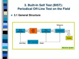
BIST Architectures • Test per scan • Test per clock • Circular self-test • Memory BIST VLSI Test: Lecture 21alt
Test Per Scan BIST PI and PO disabled during test PG Scan register Comb. logic Scan register BIST Control logic BIST enable Go/No-go signature Comb. logic Scan register Comb. logic RA Scan register VLSI Test: Lecture 21alt
Test per Clock BIST • New fault set tested every clock period • Shortest possible pattern length • 10 million BIST vectors, 200 MHz test / clock • Test Time = 10,000,000 / 200 x 106 = 0.05 s • Shorter fault simulation time than test / scan VLSI Test: Lecture 21alt
Circular Self Test VLSI Test: Lecture 21alt
Built-in Logic Block Observer (BILBO) • Combined functionality of D flip-flop, pattern generator, response analyzer, and scan chain • Reset all FFs to 0 by scanning in zeros VLSI Test: Lecture 21alt
Test per Clock with BILBO • SI – Scan In • SO – Scan Out • Characteristic polynomial: 1 + x + … + xn • CUTs A and C: BILBO1 is MISR, BILBO2 is LFSR • CUT B: BILBO1 is LFSR, BILBO2 is MISR VLSI Test: Lecture 21alt
BILBO Serial Scan Mode • B1 B2 = “00” • Dark lines show enabled data paths VLSI Test: Lecture 21alt
BILBO LFSR Pattern Generator Mode • B1 B2 = “01” VLSI Test: Lecture 21alt
BILBO in DFF (Normal) Mode • B1 B2 = “10” VLSI Test: Lecture 21alt
BILBO in MISR Mode • B1 B2 = “11” VLSI Test: Lecture 21alt
Memory BIST VLSI Test: Lecture 21alt
Summary • LFSR pattern generator and MISR response analyzer – preferred BIST methods • BIST has overheads: test controller, extra circuit delay, primary input MUX, pattern generator, response compacter, DFT to initialize circuit and test the test hardware • BIST benefits: • At-speed testing for delay and stuck-at faults • Drastic ATE cost reduction • Field test capability • Faster diagnosis during system test • Less effort to design testing process • Shorter test application times VLSI Test: Lecture 21alt