Preshower Low Voltage System Overview at CERN
This draft presents the Preshower Low Voltage System at CERN, covering Preshower structure, electronics architecture, power scenarios, cabling, and failure scenarios. It discusses regulator constraints, motherboards, current consumption, and power consumption details. The presentation highlights the geometry, control rings, and ladder prototypes in the system. Detailed information on the LV system components and their functionalities is provided by David Barney from CERN.


Preshower Low Voltage System Overview at CERN
E N D
Presentation Transcript
Preshower LV Review • Overview of presentation • Reminder of Preshower structure • Electronics architecture • Geometry • Baseline LV system • Regulator constraint and usage on different motherboards • Power-on/off scenarios • Cabling • Failure scenarios • Grounding N.B. This is a first draft of our LV system! David Barney, CERN
K chip K chip K chip K chip K chip K chip K chip K chip Readout Path FPGA DSP FED Bus Optical Receivers PACE ADC TTCrx Front End Readout ASICs DCC Slow Control & Fast Timing Signals I2C Re Clk LV1 TTCrx Control Path CCU I V I2C CCU DCU CCU CLK & T1 logic CCU CCU CCU Optoelectronics processor Link Controller TTCvimodule Front End Control ASICs Slow Control CCS Module Preshower Readout & Control Architecture All on-board ASICs are in 0.25mm technology – need 2.5V David Barney, CERN
Preshower Geometry – physical location David Barney, CERN
Preshower Geometry – envelope David Barney, CERN
20cm Preshower Geometry – internal structure David Barney, CERN
Building a ladder Prototype ladder of 8 micromodules 2003 Ladders for 7 and 10micromodules also exist Preshower geometry – mmodules and Ladders Micromodule David Barney, CERN
Motherboard Ladder completewith motherboardand cables etc. Preshower geometry – heatsinks & motherboards Add aluminium heatsinks David Barney, CERN
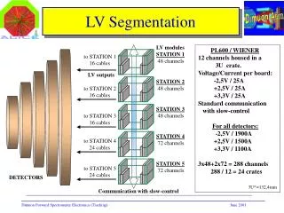
Preshower geometry – ladders & control rings A & B = motherboards (MBs)containing DOH 12 control rings / plane 1 control ring = max 12 MBs David Barney, CERN
Regulator Constraint Could load with more current if we increase Vin (i.e. drop-out voltage increases with irradiation) – but undesirable from a cooling perspective Limit maximum output current from a regulator to <2 Amps David Barney, CERN
Current consumptions from ASICs • MB type 0 = 10 PACE + 11 DCU + 5 ADC + 3 K + 3 GOH + control (no DOH) ~5 Amps • MB type 1 = 8 PACE + 9 DCU + 4 ADC + 2 K + 2 GOH + control (±DOH) ~4 Amps • MB type 2/3 = 7 PACE + 8 DCU + 4 ADC + 2 K + 2 GOH + control (no DOH) ~3.5 Amps • Should add ~20% safety margin and ~7% for current used by regulators • Variation: some type 0 and type 1 MBs contain an additional CCU as a “ring terminator”. At the moment it is unclear if this additional CCU will be powered by the board in question or an adjacent board – for redundancy considerations David Barney, CERN
Motherboard type 0 – 10 micromodules DCU used tomonitor LVRs Red = nominal (Blue) = +30% margin AR1 (Analogue Regulator #1): PACE-3, DCU and analogue part of ADC = 4xPACE + 4xDCU + 4xADCanalogue = 1160mA (1510mA) GR (GOH Regulator): for GOH + K-chip = 3xGOH + 3xK =1230mA (1600mA) DR (Digital Regulator): for Control system, QPLL and digital part of ADC = CCU + DCU + LVDSbuf+ PLL + 3xQPLL + 5xADCdigital = 815mA (1060mA) AR2 (Analogue Regulator #2): PACE-3, DCU and analogue part of ADC = 4xPACE + 4xDCU + 4xADCanalogue = 1160mA (1510mA) Total Currents Analogue: 2.9A (3.8A) Digital: 2.0A (2.7A) Total : 4.9A (6.4A) AR3 (Analogue Regulator #3): PACE-3, DCU and analogue part of ADC = 2xPACE + 2xDCU + 2xADCanalogue = 580mA (750mA) David Barney, CERN
Motherboard type 1 – 8 micromodules DCU used tomonitor LVRs Red = nominal (Blue) = +30% margin AR1 (Analogue Regulator #1): PACE-3, DCU and analogue part of ADC = 4xPACE + 4xDCU + 4xADCanalogue = 1160mA (1510mA) GR (GOH Regulator): for GOH + K = 2xGOH + 2xK =820mA (1070mA) AR2 (Analogue Regulator #2): PACE-3, DCU and analogue part of ADC = 4xPACE + 4xDCU + 4xADCanalogue = 1160mA(1510mA) DR (Digital Regulator): for control system, QPLL, DOH and digital part of ADC = CCU + DCU + LVDSbuf + PLL + 2xQPLL + 4xADCdigital + DOH = 795mA (1040mA) Total Currents Analogue: 2.3A(3.0A) Digital: 1.6A(2.1A) Total: 3.9A(5.1A) David Barney, CERN
Motherboard type 2/3 – 7 micromodules DCU used tomonitor LVRs Red = nominal (Blue) = +30% margin AR1 (Analogue Regulator #1): PACE-3, DCU and analogue part of ADC = 3xPACE + 3xDCU + 3xADCanalogue = 870mA (1130mA) GR (GOH Regulator): for GOH + K-chip = 2xGOH + 2xK =820mA (1070mA) AR2 (Analogue Regulator #2): PACE-3, DCU and analogue part of ADC = 4xPACE + 4xDCU + 4xADCanalogue = 1160mA (1510mA) DR (Digital Regulator): for control system, QPLL and digital part of ADC = CCU + DCU + LVDSbuf + PLL + 2xQPLL + 4xADCdigital = 685mA (890mA) Total Currents Analogue: 2.0A(2.6A) Digital: 1.5A(2.0A) Total: 3.5A(4.6A) David Barney, CERN
Example power consumptions per control ring 4 3 5 2 6 1 Currents in mA David Barney, CERN
Operating sequence • Constraints (some of them!): • Should power all parts of mixed-mode chips at same time • GOH (on GR) must be powered after CCU (on DR) • Inhibit lines are active HIGH at ≥2.4V (annoying!) • Need to be careful of parasitic powering effects (next slide) • Inhibit lines • Make a wire “AND” of inhibit signals from DR + ARx and take this to the outside – will refer to this as the “AND inhibit” • GOH regulator (GR) also inhibited from outside • need 24 inhibit lines per Control Ring = per LV PSU • Ideally want the LV PSU to control these inhibit lines… • Overcurrent monitoring (do we need it?) • DR is monitored externally; others monitored by CCU … David Barney, CERN
Need to be careful of parasitic powering of chips via i2c lines etc. • Chip can become powered through the clock and draw largecurrents – could result in CCU etc. being destroyed • need to include series resistors on the clock/reset lines inorder to limit the currents – but this needs to be done carefully! Operating sequence (cont.) • Power is supplied to all boards in a control ring. AND and GR are inhibited externally. • AND inhibit is disengaged – control ring comes to life, as do the PACE and ADC chips • GOH reset from CCU is asserted, the GR inhibit is released David Barney, CERN
Inhibit and overcurrent scheme (cont.) David Barney, CERN
Use of LV power supplies and LV cabling • Average current for one control ring, including ~30% margin, is ~60 Amps • Average analogue part, including 30% margin, is ~35 Amps • Average digital part, including 30% margin, is ~25 Amps • Baseline is to separate analogue and digital supplies at the power supply • According to recent news the proposed LV supply possibilities are: • 12 x 5A • 6 x 15A • 2 x 50A • 1 x 100A • Proposal is to use one 2x50A supply for each control ring • 1 channel for analogue; 1 channel for digital+control • Ideally need 24 controllable inhibit lines per supply – is this possible for the PSUs?? Otherwise we need to build a unit that can communicate with the PSU etc. • 4x16mm2 conductor for analogue, 4x10mm2 conductor for digital, per supply; - including return conductors • We have provision for ~50 wires per feedthrough : 24+few for inhibits; + 12+few for overcurrent monitoring, + DCS…. • Granularity of HV can match the LV granularity David Barney, CERN
Failure scenarios • Failure = “something” happens to a sensor or one of the chips that requires us to switch it off • Silicon sensor • Can turn-off groups of 2 sensors at the power supply end (using jumpers) and turn-off an input to the K-chip – PACE remain operational but in sleep mode • PACE, ADC or control chip • can only turn-off complete board! • unless problems with the LVDSmux are resolved we MAY lose the complete control ring! • Can also lose the complete ring if the board in question contains the ring-terminator CCU • K-chip or GOL • Will lose the data part of a board • Can maintain the control part David Barney, CERN
Grounding • General guidelines • LV supplies are floating • Every sub-detector should be electrically insulated from the others • The lead absorbers (=“structure” in the following diagrams) in the ES are the most logical pieces to define as “earth” • The ES vessel should be connected to the safety ground (Protective Earth - PE) at one single point • Each LV return should be connected to PE on the detector side • There should be a voltage limiter (~50 V) between our HV return (and cable shield) and PE on the supply side • Common return line analogue+digital from hybrid to motherboard • Motherboard layout: if possible confined (power and) ground planes analogue vs digital David Barney, CERN
LV,HV connections to PE David Barney, CERN
Pre-amp groundto Al tile PE Front-end grounding This scheme is adequate from a safety perspective David Barney, CERN
Potential problemdue to differentcable lengths… Powering scheme VERY large area ground loops! Need to test consequences….Avoiding these would be a major undertaking by CMS David Barney, CERN
PE Alternative front-end grounding 1W PE Pre-amp groundvia C to Al tile This scheme is hopefully adequate from a safety perspective David Barney, CERN
Alternative powering scheme David Barney, CERN
Summary • We have tried to develop a baseline LV scheme that has as much flexibility as possible, given certain constraints • There are some questions that need to be addressed seriously: • Maximum number of controllable inhibit lines per LV PSU – is 24 possible? • Parasitic powering of chips via i2c lines etc. • Details, details, details! • In the coming months we will try to resolve as many issues as possible, and test a variety of powering/grounding schemes. • There are many unverified parts of our system (particularly in the grounding scheme). We will not have all the answers before the cables need to be laid in 2004 David Barney, CERN
Backup slides David Barney, CERN
DOH A A A A A A A A Control Ring chipset Control Ring chipset Control Ring chipset Control Ring chipset I V I V I V I V B B B B B B B B Token ring tests (cont.) • 1 board (=no “ring”) runs for ever with no serious problems • 4 boards in a ring can run for ever (some modifications to the C++ code were necessary to remove “tracker” specifics) • 4 boards, with one board bypassed (redundancy in operation) powered, runs ok • As above but with the “bad” board powered down (PD) causes fatal errors – not yet fully understood • Errors reported in the two boards following the one that is powered-down • The LVDS output lines from the PD board are floating – and the LVDSmux chip is susceptible to noise (no hysteresis pads) • More tests planned with dedicated boards…. • …and more tests when we get the real system boards David Barney, CERN
Supplies/channels/feedthroughs David Barney, CERN
Power Supply - + R2=2*R1 R3=3*R1 Ir tot=3*I If tot=3*I U1 R1 RL I I1=I+I1’=I*(18/11) I1’=I2’+I3’=I*(8/11) I1 I1=I*(18/11) I2=I*(9/11) I3=I*(6/11) R2 RL I U=U2-U1 I2 I2’=I*(2/11) R3 RL I I3 I3’=I*(5/11) U2 David Barney, CERN
Motherboard type 0 – 10 micromodulesalternative scheme DCU used tomonitor LVRs Red = nominal (Blue) = +30% margin AR1 (Analogue Regulator #1): PACE-3, DCU and analogue part of ADC = 4xPACE + 4xDCU + 4xADCanalogue = 1160mA (1510mA) GR (GOH Regulator): GOH + digital part of ADC = 3xGOH + 5xADCdigital =980mA (1280mA) DR (Digital Regulator): for Control system and K-chip = CCU + DCU + LVDSbuf + PLL + 3xK + 3xQPLL = 1065mA (1390mA) AR2 (Analogue Regulator #2): PACE-3, DCU and analogue part of ADC = 4xPACE + 4xDCU + 4xADCanalogue = 1160mA (1510mA) Total Currents Analogue: 2.9A (3.8A) Digital: 2.0A (2.7A) Total : 4.9A (6.4A) AR3 (Analogue Regulator #3): PACE-3, DCU and analogue part of ADC = 2xPACE + 2xDCU + 2xADCanalogue = 580mA (750mA) David Barney, CERN
Motherboard type 0 – 10 micromodulesIf the CCU could be used to control regulators DCU used tomonitor LVRs Red = nominal (Blue) = +30% margin AR1 (Analogue Regulator #1): PACE-3, DCU and analogue part of ADC = 4xPACE + 4xDCU + 4xADCanalogue = 1160mA (1510mA) CR (Control Regulator): control system + GOH = DCU + CCU + LVDSbuf + PLL + 3xGOH =705mA (920mA) DR (Digital Regulator): for K-chip, QPLL and digital part of ADC = 3xK + 3xQPLL + 5xADCdigital = 1340mA (1740mA) AR2 (Analogue Regulator #2): PACE-3, DCU and analogue part of ADC = 4xPACE + 4xDCU + 4xADCanalogue = 1160mA (1510mA) Total Currents Analogue: 2.9A (3.8A) Digital: 2.0A (2.7A) Total : 4.9A (6.4A) AR3 (Analogue Regulator #3): PACE-3, DCU and analogue part of ADC = 2xPACE + 2xDCU + 2xADCanalogue = 580mA (750mA) David Barney, CERN
Motherboard type 1 – 8 micromodulesalternative scheme DCU used tomonitor LVRs Red = nominal (Blue) = +30% margin GR (GOH Regulator): for GOH + digital part of ADC = 2xGOH + 4xADCdigital =720mA (940mA) AR1 (Analogue Regulator #1): PACE-3, DCU and analogue part of ADC = 4xPACE + 4xDCU + 4xADCanalogue = 1160mA (1510mA) AR2 (Analogue Regulator #2): PACE-3, DCU and analogue part of ADC = 4xPACE + 4xDCU + 4xADCanalogue = 1160mA(1510mA) DR (Digital Regulator): for control system, K-chip, QPLL and DOH = CCU + DCU + PLL + LVDSbuf + 2xK + 2xQPLL + DOH = 900mA (1160mA) Total Currents Analogue: 2.3A(3.0A) Digital: 1.6A(2.1A) Total: 3.9A(5.1A) David Barney, CERN
Motherboard type 1 – 8 micromodulesif CCU could be used to control regulators DCU used tomonitor LVRs Red = nominal (Blue) = +30% margin CR (Control Regulator): control system + GOH = DCU + CCU + LVDSbuf + PLL + DOH + 2xGOH =655mA (850mA) AR1 (Analogue Regulator #1): PACE-3, DCU and analogue part of ADC = 4xPACE + 4xDCU + 4xADCanalogue = 1160mA (1510mA) AR2 (Analogue Regulator #2): PACE-3, DCU and analogue part of ADC = 4xPACE + 4xDCU + 4xADCanalogue = 1160mA(1510mA) DR (Digital Regulator): for K-chip, QPLL and digital part of ADC = 2xK + 2xQPLL + 4xADCdigital = 960mA (1250mA) Total Currents Analogue: 2.3A(3.0A) Digital: 1.6A(2.1A) Total: 3.9A(5.1A) David Barney, CERN
Motherboard type 2/3 – 7 micromodulesalternative scheme DCU used tomonitor LVRs Red = nominal (Blue) = +30% margin AR1 (Analogue Regulator #1): PACE-3, DCU and analogue part of ADC = 3xPACE + 3xDCU + 3xADCanalogue = 870mA (1130mA) GR (GOH Regulator): for GOH + digital part of ADC = 2xGOH + 4xADCdigital =720mA (940mA) AR2 (Analogue Regulator #2): PACE-3, DCU and analogue part of ADC = 4xPACE + 4xDCU + 4xADCanalogue = 1160mA (1510mA) DR (Digital Regulator): for control system, K-chip, QPLL = CCU + DCU + LVDSbuf + PLL + 2xK + 2xQPLL = 785mA (1020mA) Total Currents Analogue: 2.0A(2.6A) Digital: 1.5A(2.0A) Total: 3.5A(4.6A) David Barney, CERN
Motherboard type 2/3 – 7 micromodulesif CCU could be used to control regulators DCU used tomonitor LVRs Red = nominal (Blue) = +30% margin AR1 (Analogue Regulator #1): PACE-3, DCU and analogue part of ADC = 3xPACE + 3xDCU + 3xADCanalogue = 870mA (1130mA) CR (Control Regulator): control system + GOH = DCU + CCU + LVDSbuf + PLL + 2xGOH =545mA (710mA) AR2 (Analogue Regulator #2): PACE-3, DCU and analogue part of ADC = 4xPACE + 4xDCU + 4xADCanalogue = 1160mA (1510mA) DR (Digital Regulator): for K-chip, QPLL and digital part of ADC = 2xK + 2xQPLL + 4xADCdigital = 960mA (1250mA) Total Currents Analogue: 2.0A(2.6A) Digital: 1.5A(2.0A) Total: 3.5A(4.6A) David Barney, CERN