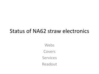
Advanced Electronic System for NA62 Gigatracker at CERN
160 likes | 253 Vues
This paper presents the cutting-edge electronics system for the NA62 Gigatracker, including specifications, setup, configuration, and data rate details. The system features jitter-free pixel signals, time-to-digital conversion, grouping of pixels, and transmission lines.

Advanced Electronic System for NA62 Gigatracker at CERN
E N D
Presentation Transcript
The NA62 Gigatracker electronics presented by A. Kluge CERN/PH-ESE Nov 22, 2011 A. Klugea, G. AglieriRinellaa, V. Carassitic , A. Ceccucci, E. Cortina, J. Daguin, G. Dellacasab, M. Fiorinia, S. Garbolinb, P. Jarrona, J. Kaplona, F. Marchettob, E. Martina,d, A. Mapellia,e, G. Mazzab, M. Morela, M. Noya, G. Nüssle, P. Petagna, L. Perktolda, A. Cotta Ramusinoc, P. Riedlera, A. Rivettib, R. Wheadonb a CERN, Geneva Switzerland, bINFN Torino, Italy, cINFN Ferrara, Italy, dUCL Louvain la Neuve, Belgium, dEPFL LausanneSwitzerland
Experimental setup: GTK specifications 200 ps per station 300 µm 100 pstime binning of arrival time 300 µm 800 MHz particle rate A. Kluge
Experimental setup: GTK specifications 300 µm thin, 200µm sensor + 100 µm chip(<0.5% of X0), operated in vacuum 100 pstime resolution arrival time 300 µm A. Kluge
Beam & detector configuration A. Kluge
Beam profile 60 mm 27 mm A. Kluge
ASIC covering beam 60 mm 12 mm 4.5-6 mm 13.5 mm 27 mm 45 rows times 40 columns per chip = 1800 pixels per chip A. Kluge
Configuration for beam 27-60 A. Kluge
Data rate • Rate of center column = chip design rate: 3.3 MHz/column ~ 82 MHz/cm2 • => avg rate 73 kHz/pixel • => 132 MHz/chip • => 132 MHz/chip * ~ 32 bit = ~4.2 Gbit/s • => max rate in beam center 140 kHz/pixel • Data word length 32 or 41 bit 12 mm 13.5 mm A. Kluge
Jitter-free pixel signal to TDC in EOC amplifier & discriminator/time-walk-compensator reference clock time-to-digital converter TDC buffering & read-out processor A. Kluge
The time-to-digital conversion Delay locked loop based TDC A. Kluge
DLL based TDC Pixel cell DAC1 Ref CLK Phase detector & charge pump UP VCTRL PD CP 0 1 2 m-2 m-1 DOWN DLL CLK Clk = tclk TDC A. Kluge
grouping of pixels TOT discriminator pre-amplifier transmission line driver 5 transmission lines Pixel cell 0 Pixel cell 10 Pixel cell 20 TDC bank Pixel cell 30 Pixel cell 40 5 transmission line receivers A. Kluge
45 45 45 45 45 40 Hit Arbiter Hit Arbiter Hit Arbiter Hit Arbiter Addr. Addr. Addr. Addr. 32 Hit Reg2 Hit Reg1 Hit Reg2 Hit Reg1 Hit Reg2 Hit Reg1 Hit Reg2 Hit Reg1 LVDS Ref CLK 320MHz DLL Digital processing serializer 45 x 40 pixel final chip