Download
1 / 22
220 likes | 338 Vues
Readout electronics of the NA62 Gigatracker system.

E N D
Readout electronics of the NA62 Gigatracker system G. Dellacasa1, V.Carassiti3, A. Ceccucci2, S. Chiozzi3, E. Cortina4, A. Cotta Ramusino3, M. Fiorini2, S. Garbolino1, P. Jarron2, J. Kaplon2, A. Kluge2, F. Marchetto1, S. Martoiu1, E. Martin Albarran4, G. Mazza1, M. Noy2, F. Petrucci3, P. Riedler2, A. Rivetti1, S. Tiuraniemi2, R. Wheadon1 (1) I.N.F.N. Torino (2) CERN (3) I.N.F.N. Ferrara (4) Louvain la Neuve ICATPP 2009 Villa Olmo – Como
Outline • Gigatracker system overview • Readout architectures: two possible solutions: • On-pixel TDC demonstrator ASIC • End-of-Column TDC demonstrator ASIC • Conclusions Giulio Dellacasa
Experimentalapparatus Measure position Identifies π Hit correlation ~ 100 ps Select particles with 75 GeV/c GTK sees all particles 20% of the K+ decays in the vacuum region of which only one out of 10-11 is of interest (pi+nu nu br) Giulio Dellacasa
Gigatracker Overview • NA62 Gigatracker (GTK) consists of three silicon pixel stations installed over the beam line. It will provide several measurements of the beam particles (K+): timing, direction, momentum • Each station cover an area of 60(X) x 27(Y) mm2.Each pixel 300 μm x 300 μm • The maximum beam particle intensity it will be ~1.5 MHz/mm2 (1 GHz over the whole detector, thus the name Gigatracker) • The required track time resolution is ~ 200 ps (rms) per station (~ 150 ps the whole GTK) and space resolution ~ 100 μm (rms) over the whole system • A material budget of 0.5% X0 is target for each pixel station (sensor thickness : 200 μm, readout chip thickness : 100 μm) A1÷A4: dipole magnets to provide the momentum selection and recombination Giulio Dellacasa
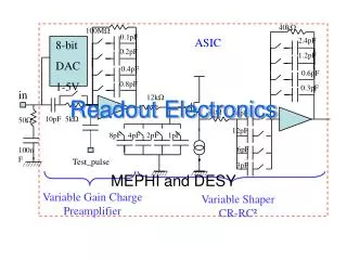
Gigatracker readout • Two rows of five readout chips (0.13 μm CMOS technology) are bump bonded to the sensor elements. Each chip reads a matrix of 40x45 pixels • Maximum particle intensity per chip: 130 MHz • Maximum particle intensity per pixel: 140 kHz • Total average data rate per chip: 4.2 Gb/s (6 Gb/s with fluctuations) • Total dose in 1 year: 105 Gy. Thus the system should be cooled at 5 oC or less and GTK stations replaced after a runtime of 60 days under optimum beam conditions • Dissipated heat produced by the 10 readout chips must be lower than 2 W/cm2 (32 W in total) Pixel matrix Readout chip Mechanical support Giulio Dellacasa
Time walk correction • With a dynamic range 10:1 and a resolution requirement of 200 ps per station (100 ps per chip for safety), a time walk compensation has to be applied • Low Power Constant Fraction Discriminator (CFD): analogue signal processing technique • Only one time measurement per hit • Analogue design more complicated • Time Over Threshold (ToT): time walk correction is based on an algorithm derived from the correlation between the ToT (pulse width) and the experienced time walk. • Two time measurements per hit (rising and falling edges) • Accurate calibration of the system is required to define the correction algorithm Giulio Dellacasa
TDC options • In the chip a clock counter will provide a coarse time information. A fine measurement will be obtained with a Time to Digital Converter (TDC) • The dynamic range of the TDC should span 2 clock cycles, to avoid ambiguities • Time to Amplitude Converter (TAC) and Delay Locked Loop (DLL) based TDCs can be developed • A TAC based TDC can be implemented on each pixel • The comparator signal does not need to be propagated outside the pixel • More noise problems inside the cell • Must be designed to be radiation-tolerant (total dose and SEU aspects), due to the high radiation dose received in the pixel area • A DLL based TDC is faster, so it will be used if the TDC will be shared among different pixels • The comparator signal needs to be propagated outside the pixel (transmission line problems) • Dead time in case of multiple hits in the same pixels group Giulio Dellacasa
Readout architectures • Two different architectures for the GTK readout chip are under development: • Time walk correction using a CFD filter + TDC on pixel based on TAC (On-pixel TDC option) • Time walk correction using ToT technique + TDC based on DLL shared among a group of pixels (End of Column TDC option) • For both architectures one demonstrator chip has been submitted at the end of March. Test are ongoing in order to evaluate their performance and feasibility for the final readout option Giulio Dellacasa
On-pixel TDC architecture’s prototype Giulio Dellacasa
The pixel cell • The time-walk correction is performed by a CFD filter and the time measurement is provided by a Time to Amplitude Converter (TAC) based on a Wilkinson ADC. Both CFD and TDC are implemented on each pixels cell • The discriminated signal (CFD output) is used to store the value of the Time Stamp (10-bit bus +1, 160 MHz clock) • The fine time information is measured by starting a calibrated voltage ramp at the CFD rising edge and stopping it at the next clock rising edge. The measure of the voltage reached by the ramp gives the timing distance between the incoming signal and the clock rising edge. The obtained voltage is therefore converted by a Wilkinson ADC (7 bit + 1 bit overlapping) • TDC time binning: 12.5 / 128 ns = 97.6 ps (clock freq/2) • Derandomization is performed in the pixel cell • Exhaustive simulations have been performed to calculate the correct FIFO depths and to evaluate the impact of the pixel dead time (< 0.2% lost events at 140 kHz ) Giulio Dellacasa
End of Column controller • Each column of 45 pixels is readout by its own controller (End of Column controller) • 40 EoC controller in the final readout chip • One single Coarse Counter for the whole ASIC (Gray counter) • Only digital buses between pixels and EoC controller • End of Column controller provides data formatting. Data stored in the output buffer are grouped in Frames • Definition of Frame: all the data which belong to the same turn of the Coarse Counter (6,4 μs) • 32 bit per hit: Addresses + Coarse measure + Fine measure • CRC control added in trailer (CRC-16 polynomial is X16+X15+X2+1) Giulio Dellacasa
On-pixel TDC demo ASIC • The demonstrator chip is organized in two folded columns of 45 pixels and one smaller column with only 15 pixels (plus spare pixels for testing). • For each of them a totally independent End-of-Column Controller is responsible to readout data, adding additional informations before to send them out via a serial shift register Giulio Dellacasa
On-pixel TDC layout Digital pads Analogue pads Clk drivers Analogue test pads End of Column Logic 2 test pixels Digital test pads Pixel matrix1 x 15 cells columns Pixel matrix2 x 45 cells columns 5 x 4 mm Giulio Dellacasa
On-pixel TDC Demo chip • CMOS 130 nm • 5 mm x 4 mm • 118 bonding wire pads • 106 bump bonding pads (sensor) • 105 + 2 pixel cells • LVDS interface • 1.2 V core supply • SEU protection both in the pixel cells and the End of Column controller performed by Hamming encoding for registers and FSMs (single error correction, double error detection) • ASIC has been submitted at the end of march • Testing: Production of the test board PCB just started Giulio Dellacasa
End of column TDC architecture’s prototype Giulio Dellacasa
Each pixel cell is equipped with a preamplifier and Time Over Threshold discriminator ToT output has a constant amplitude and a pulse width proportional to the input charge. It is transmitted to the End-Of-Column circuit Pulse width is used to correct the time walk EoC circuit contains all the rest of processing functions: time stamping with the TDC, pixel address encoding, data pipelining and formatting The pixel cell Giulio Dellacasa
Architecture overview (45 x 40 final chip) Giulio Dellacasa
EoC TDC Demo chip • Demo chip has 60 pixels divided up into 3 groups: • Main array: 45 pixels with 9 EoC readout blocks, each one serving the 5 pixels through the arbiter block • Small array: 9 pixels, each driving a different EoC block. There is no hit arbiter block here • Test column: 6 pixels with analog output • Hit Arbiter: defines first arriving pixels out of 5 (asynchronous latch) • Coarse time information is provided by 32-bit counters hosted in the EoC logic • TDC information (fine time) is encoded in 32-bit words. In order to reduce the amount of data to transmit 32 to 5 bit encoders will be used in the final version Giulio Dellacasa
TDC architecture • Coarse time information provided by 32-bit counters (320 MHz) hosted in the EoC. (Rising and falling edge for both clock and hit) • Fine time information provided by TDC • In order to reduce dead time and to reach the efficiency of 99%, the use of a fast TDC is mandatory. So a DLL based TDC will be adopted • Reference clock: 320 MHz (3.125 ns) • DLL consists of 32 delays elements, 100 ps delay each • 2 hit registers (with 5-bit encoder) to provide rising and falling edges of the ToT pulse (not implemented in the demonstrator chip) Giulio Dellacasa
End of Column TDC layout • ASIC has been submitted at the end of march (130 nm CMOS technology) • Analog test just started Giulio Dellacasa
Theoretical Comparison table Giulio Dellacasa
Conclusions • Gigatracker system is very challenging due the high rate and the required time resolution of 150 ps • Both proposed architectures have advantages and disadvantages • Test and measurements of the two different prototypes will give an experimental result to compare the two possible solutions • First results soon! Giulio Dellacasa