
Datapath and Control
E N D
Presentation Transcript
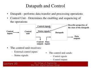
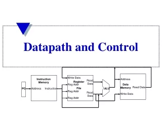
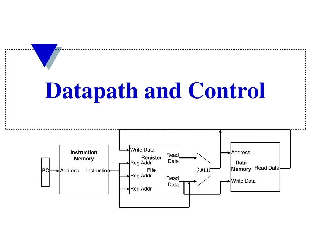
Write Data Instruction Memory Address Read Data Register File Reg Addr Data Memory Read Data PC Address Instruction ALU Reg Addr Read Data Write Data Reg Addr Datapath and Control
Single Cycle Implementation Cycle Time • Unfortunately, though simple, the single cycle approach is not used because it is inefficient • Clock cycle must have the same length for every instruction • What is the longest path (slowest instruction)? • Calculate cycle time assuming negligible delays (for muxes, control unit, sign extend, PC access, shift left 2, wires) except: • Instruction and Data Memory (2ns) • ALU and adders (2ns) • Register File access (reads or writes) (1ns) • floating point operations even longer
What about floating point operations? • A floating point add.d = Instr. Fetch (2 ns)+ Reg. Read (1 ns)+ ALU add(8 ns)+ Reg. Write (1 ns)= 12 ns • Floating point load l.s=2+1+2(ALUop)+2(data mem)+1 (Reg.) = 8 ns • Floating point store s.s =2+1+2(ALU)+2(data mem) = 7 ns. • The longest instruction is floating point multiply mul = Inst. Fetch (2 ns)+Reg. Read (1 ns)+ALU multiply (16 ns)+ Reg. Write (1 ns) = 20 ns • Floating point branch = 5 ns, floating point jump=2 (fetch) • If clock period is variable in length, then we need to look at instruction frequency. For example Loads (31%), stores (21%), R-type (27%), beq(5%), j (2%), add.d, sub.d (7%), mult.d, div.d(7%). • Combining to compute the clock cycle=8x31%+7x21%+6x27%+5x5%+2x2%+20x7%+12x7%= 7 ns
What about variable cycle length? • Instead of a fixed cycle time, we allow cycle time to depend on instruction class. • We can then compare performance, considering that CPI will still be 1, and Instruction count does not change. Perf. CPU variable cycle time = CPU exec. time fixed cycle time Perf. CPU fixed cycle time CPU exec. time var. cycle time = Clock period fixed Clock period variable • because performance= _____________1______________ ) Instr. Count x CPI x Clock Period • Performance improvement = 20 ns (fixed cycle clock period) = 2.86 faster 7 ns (variable cycle clock period)
Where We are Headed • Single cycle/instr. uses the clock cycle inefficiently – the clock cycle must be timed to accommodate the slowest instruction – we cannot make common case fast. • especially problematic for more complex instructions like floating point multiplications • Single cycle/instr. datapath is wasteful of area since some functional units must be duplicated since they can not be “shared” during an instruction execution • e.g., need separate adders to do PC update and branch target address calculations, as well as an ALU to do R-type arithmetic/logic operations and data memory address calculations
IR Address Memory A Read Addr 1 PC Read Data 1 Register File Read Addr 2 Read Data (Instr. or Data) ALUout ALU Write Addr Write Data Read Data 2 B Write Data MDR Where We are Headed • Another approach • use a “smaller” cycle time • have different instructions take different number of cycles • a “multi-cycle” datapath
Multicycle Implementation Overview • Each step in the execution of an instruction takes 1 clock cycle • An instruction takes more than 1 clock cycle to complete • Not every instruction takes thesame number of clock cycles to complete • Multi-cycle implementations allow functional units to be used more than once per instruction as long as they are used on different clock cycles, as a result • we need only one memory • we need only one ALU/adder • We can have faster clock rates
IR Address Memory A Read Addr 1 PC Read Data 1 Register File Read Addr 2 Read Data (Instr. or Data) ALUout ALU Write Addr Write Data Read Data 2 B Write Data MDR The Multicycle Datapath – A High Level View • Registers have to be added after every major functional unit to hold the intermediate output value until that intermediate result is used in a subsequent clock cycle
The Multicycle Datapath – A High Level View • All internal registers hold the intermediate output value until it is used in a subsequent clock cycle of that instruction, thus do not need a dedicated control signal. • The only exception is the Instruction Register (IR), which needs to hold the instruction bits for several cycles, until the instruction finishes its execution. • Thus it needs a control signal which allows it to be written into - IRWrite • Data used by subsequent instructions are stored in programmer visible elements (like Register File, PC or memory)
Multicycle Approach • Break up the instructions into steps where each step takes a cycle while trying to • balance the amount of work to be done in each step • restrict each cycle to use only one major functional unit • Thus each cycle can at most do one of the following operations • a memory access or • a register file access (two reads or one write), or • an ALU operation
System Clock clock cycle IRWrite MemWrite RegWrite IR Address Memory Read Addr 1 A PC Read Data 1 Register File Read Addr 2 Read Data (Instr. or Data) ALUout ALU Write Addr Write Data Read Data 2 B Write Data MDR simplified Clocking the Multicycle Datapath
Multicycle Approach, continued • Reading/writing to any of the internal registers (except IR) or to the PC occurs (quickly) at the end of a clock cycle • reading/writing to the register file takes ~50% of a clock cycle since it has additional control and access overhead (reading can be done in parallel with instruction decode) • All operations occurring in one step occur in parallel within the same clock cycle • This limits us to one ALU operation, one memory access, and one register file access per step (per clock cycle)
IR Address Memory A Read Addr 1 PC Read Data 1 Register File Read Addr 2 Read Data (Instr. or Data) ALUout ALU Write Addr Write Data Read Data 2 B Write Data MDR The Multicycle Datapath – A High Level View • Need more multiplexors to direct the datapath to fewer logical units
IorD PC 0 ALUSrcA 1 PC Address Memory 0 A 1 zero ALUOut Read Data (Instr. or Data) ALUout ALU Multiplexors used in multicycle datapath • The first multiplexor determines whether memory address input comes from the PC (for instruction fetching) or from the ALU (for lw, swinstructions) • The second multiplexor determines whether input to the ALU first port is from internal register A (during R-type operations for example), or from the PC (to compute the next PC value).
ALUSrcB zero 2 ALU B 0 Instr[15-0] Sign Extend 4 1 32 2 Shift left 2 3 Multiplexors used in multicycle datapath • The third multiplexor determines whether input to the ALU second port comes from Internal register B (for R-type instructions), a constant 4 (to increment the PC), the sign-extended Instruction [15-0] bits (for immediate operations), or those bits shifted left by 2 (for branch operations)
ALU zero output PCSouorce PCWriteCond PC[31-28] 2 PCWrite Instr[25-0] Shift left 2 28 2 (PC+4)ALU result 0 PC 1 ALUout Multiplexors used in multicycle datapath • The fourth multiplexor determines the address of the destination register in the Register File, whether input comes from Instr[20-16] bits or from Instr[15-11] bits (this is the same with the single-cycle/instruction datapath. • Another multiplexer determines whether data to be written in the Register File comes from the Memory Data Register or from ALUout. • Finally, there is a four-way multiplexor to determine what is written into the PC. Its control signal is PCSource
PCWriteCond PCWrite PCSource IorD ALUOp MemRead Control ALUSrcB MemWrite ALUSrcA MemtoReg IRWrite RegDst RegWrite PC[31-28] Instr[31-26] Shift left 2 28 Instr[25-0] 2 0 1 Address Memory 0 PC 0 Read Addr 1 A IR Read Data 1 Register File 1 1 zero Read Addr 2 Read Data (Instr. or Data) 0 ALUout ALU Write Addr Write Data 1 Read Data 2 B 0 1 Write Data 4 1 0 2 MDR Instr[15-0] Sign Extend Shift left 2 3 32 ALU control Instr[5-0] The Complete Multicycle Data with Control