Perfect and Affordable Wafer
20 likes | 45 Vues
A semiconductor is a critical and integral part utilized in every electronic device to operate efficiently. Knowing a procedure before owning can help to determine an ideal material. Want to know more? Ping us an email at sales@waferworld.com.

Perfect and Affordable Wafer
E N D
Presentation Transcript
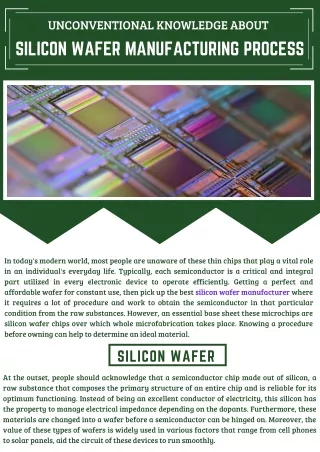
UNCONVENTIONAL KNOWLEDGE ABOUT SILICON WAFER MANUFACTURING PROCESS In today's modern world, most people are unaware of these thin chips that play a vital role in an individual's everyday life. Typically, each semiconductor is a critical and integral part utilized in every electronic device to operate efficiently. Getting a perfect and affordable wafer for constant use, then pick up the best silicon wafer manufacturer where it requires a lot of procedure and work to obtain the semiconductor in that particular condition from the raw substances. However, an essential base sheet these microchips are silicon wafer chips over which whole microfabrication takes place. Knowing a procedure before owning can help to determine an ideal material. SILICON WAFER At the outset, people should acknowledge that a semiconductor chip made out of silicon, a raw substance that composes the primary structure of an entire chip and is reliable for its optimum functioning. Instead of being an excellent conductor of electricity, this silicon has the property to manage electrical impedance depending on the dopants. Furthermore, these materials are changed into a wafer before a semiconductor can be hinged on. Moreover, the value of these types of wafers is widely used in various factors that range from cell phones to solar panels, aid the circuit of these devices to run smoothly.
MANUFACTURING PROCESS Most likely, it begins with the extraction of silicon so, there is no wafer without perfect silicon. People might be surprised when it comes to knowing that these wafers are extracted from silica sand. Further, it is in the natural state so, it needs too much oxygen to convert. Thus, the material is combined with carbon and burned in an electric furnace to a temperature above 2000 degrees Celcius. During this stage, chemical element separates the pollutants like calcium or aluminum. PURIFICATION Once the silicon is extracted, it can be purified by the using an extensive technical process such as a ground down to a fine powder, and then merged with hydrogen chloride along with heating, which creates a perfect 100% purified silicon. SLICING & POLISHING After purification, the fairly pure ingot needs to slice into equal wafers with diamond cut edged saw blades. Each work is vital to get more effective so, professionals polish it with a device that produces a mirror-like structure. Finally, it can be cleaned and tested which helps to obtain the potent and efficient wafer that provides high stability. (561) 842-4441 West Palm Beach, FL @ Waferworld @ WaferWorldInc