non linear
E N D
Presentation Transcript
PULSEANDDIGITALCIRCUITS (A40415) II-B.TechII- Sem-ECE (R15Regulation) Preparedby B.Naresh Asst.Prof
UNIT-1 LINEARWAVESHAPING
Basics AnalogQuantities • Most natural quantities that we see are analog and vary continuously.Analogsystemscangenerallyhandlehigher powerthandigitalsystems Temperature (F) 100 95 90 85 80 75 70 Timeofday 1 2 3 4 5 6 7 8 9 101112 1 2 3 4 5 6 7 8 9 101112 • Digitalsystemscan Ap.Mr.ocess,store, anP.Md.transmitdatamore efficientlybutcanonlyassigndiscretevalues to eachpoint
AnalogandDigitalSystems • Digitalsystemscanprocess,store,andtransmitdata more • efficientlybutcanonlyassigndiscretevaluesto eachpoint CDdrive 10110011101 Digitaldata Digital-to-analog converter Linearamplifier Analog reproduction ofmusicaudio signal Speaker Sound waves
Contd.. • Digitalelectronicsusescircuitsthathavetwostates,whichare represented by twodifferentvoltagelevelscalledHIGHand LOW. Thevoltagesrepresentnumbersinthebinarysystem • Inbinary,asinglenumberiscalled abit(forbinarydigit).A bitcanhavethe value ofeither a0 ora1, depending on ifthe voltageisHIGHorLOW. V H(max VH(min VL(max VL(min)
DigitalSignals • DigitalwaveformschangebetweentheLOW andHIGH levels.Apositivegoingpulseisonethat goesfrom anormally LOWlogiclevelto aHIGHlevelandthenbackagain.Digital waveformsaremadeup ofaseries ofpulses HIGH HIGH Risingor leadingedge Fallingor leadingedge Fallingor trailingedge Risingor trailingedge LOW LOW t t t t 0 1 0 1 (a)Positive–goingpulse (b)Negative–goingpulse
PulseDefinitions • Actualpulsesarenot idealbut aredescribedbytherise time,falltime,amplitude,andothercharacteristics. Overshoot Ringing Droop 90% tW Pulsewidth Amplitude 50% 10% Ringing Baseline Undershoot tr tf Risetime Falltime
PeriodicPulseWaveforms • Periodicpulsewaveformsarecomposedofpulses thatrepeatsinafixedintervalcalledtheperiod. • The frequency is the rate it repeats and is measured in hertz. The clock is a basic timing signal that is an exampleofaperiodicwave. • • • T1z • f • Whatisthe periodofarepetitivewaveiff= 3.2GHz?
PulseDefinitions • Inadditionto frequencyandperiod,repetitivepulse waveformsaredescribedbythe amplitude(A),pulsewidth (tW)and dutycycle.Duty cycleistheratiooftWtoT. Volts Pulse width Amplitude (tW) Time Period, T
WaveShaping Definition: It is the process of changing the shapeofinputsignal with linear/non-linear circuits. Types: LinearWaveShaping Non-linearWaveShaping
LinearWaveShaping Definition:Theprocesswhereby theformofa non-sinusoidal signal is changed by transmission through a linear network is called Linear Wave Shaping. Types: HighPass RCCircuit. LowPassRCCircuit.
Non-sinusoidalwaveforms Step Pulse Squarewave Ramp Exponentialwaveforms.
StepWaveform A step voltage is one which maintains the value zero for all times t<0 and maintainsthevalueVforalltimest>0. Vi V Vi=0 t<0 V=V t>0 i t t=0 Pulse Thepulseamplitude is„V‟andthepulsedurationistp. Vi V 0≤t≤tp Vi=V Vi=0 Otherwise t 0 t=0 t=tp
SquareWave • A wave form which maintains itself at one constant level v1 for a time T1 andatotherconstantLevelV11foratimeT2andwhichisrepetitivewith aperiodT=T1+T2is calledasquare-wave. T2 T1 Ramp Awaveformwhichiszerofort<0andwhichincreaseslinearly withtimefort>0. Vi Vi=αt Vi=αt, t>0 t 0
Exponential • Theexponentialwaveforminputisgivenby • whereTisthetimeconstantoftheexponentialinput • Vi • V t 0
HighPassRCCircuit C + + 1 2fC XC R V V i o - - Iff=low, Xcbecomeshigh C actasopencircuit,sotheVo=0. Iff=high,Xcbecomeslow C actsasshort circuit,sowegettheoutput. Thehigherfrequencycomponentsintheinputsignal appear at the output with less attenuation due to this behavior thecircuitiscalled“HighPassFilter”.
Sinusoidalinput • ForSinusoidalinput,theoutputincreasesin amplitudewithincreasingfrequency. • C Vo=iR + + R i V V Vin _ V in R-jXC in j i= = R- 2πfC _ O Vin i= j R1- 2πfRC Vin×R Vin V=iR= = j O j 1- 2πfRC R1-2πfRC
VO 1 = Vin 1+j-f1 f VO Vin 1 = A0.707 2 f1 1+ f θ=-tan-1-f1=tan-1f1 ff At thefrequencyf=f1 VO= 1 =1=0.707 1+1 2 Vin
Atf=f1thegainis0.707orthislevelcorrespondstoasignalreductionof3Atf=f1thegainis0.707orthislevelcorrespondstoasignalreductionof3 decibels(dB). f1 isreferredtoasLower3-dBfrequency.
Squarewaveinput • PercentageTilt(00Tilt) • Tiltisdefinedasthedecay intheamplitudeof theoutputvoltagewavedue totheinputvoltagemaintainingconstantlevel VV1 P 1 1 V X100 2 -T1 ' 1 V (1) = V1.e RC -T2 ' 2 V (2) =V2 .e RC - V = V V -V' =V 1 2 ' 1 V (3) 2 (4)
AsymmetricalsquarewaveisoneforwhichT1=T2= • symmetryV1=-V2 • Bysubstituting theseinaboveequation(3) &becauseof • -T2RC- V=V1.eV2 -T2RC+ V=V1.e V1 -T2RC V=V1(1+e) I Equation(1) II
ForRC>>T theequation(I)&(II)becomesas 2 V1V(1+T )&V1V(1- T ) 1 2 4RC 2 4RC V1-V1 Thepercentagetilt‘P’isdefinedbyP= 100 1 V 2
HighPassRCcircuitactsas differentiator:- • The timeconstantof highpassRCcircuitinverysmallincomparison withinthetimerequired fortheinputsignaltomakeanappreciable change,thecircuit iscalleda“differentiator”. • Under thiscircumstancesthevoltagedropacrossRwillbeverysmallin comparison withthedropacrossC. Hencewemay considerthatthe totalinputViappearsacross C,sothatthecurrentisdeterminedentirely bythecapacitance. • Thenthecurrent isi=C • V0=iR • V0=RC andtheoutput signalacross Ris • hencetheoutput is proportionaltothe derivativeoftheinput.
LowPassRCCircuit 1 X C 2f C Iff=low, Xcbecomeshigh C actasopencircuit,sowegettheoutput. Iff=high,Xcbecomeslow C actsasshortcircuit,soVo=0. Asthe lowerfrequencysignalsappearattheoutput,itiscalledas “LowpassRCcircuit”.
Sinusoidalinput V 1i o CS ×XC V in j XC V = O R+ j 1 2fC wh X= ere C 1 jC 1 × V in V = O R+ jC Vin Vin V= = O jRC+1 1+j2fRC
Vin 1 2RC V= O wheref= 1+jf 2 f 2 1 = A= VO Vin f f2 1+j = 1 and θ=-tan-1f f A 2 2 1+f f 2 At thefrequencyf=f2 VO= 1 =1=0.707 1+1 2 Vin A0.707
Atf=f2thegainis0.707orthislevelcorrespondstoasignalreductionof3 decibels(dB). f2 orfh isreferredtoas upper3-dBfrequency.
Squarewaveinput • RiseTime(tr): • The time required for the voltage to rise from 10 9000ofthefinalsteadyvalueiscalled“RiseTime”. 00to V’ V’ V2 V2 V01 Vd.c. V02 V’’ T2 V1 T1
=V1 +(V1-V1). e-T1RC Theoutput voltageV01&V02isgivenby V01 …………………(1) …………………(2) V =V11+(V2-V11).e-T2RC 02 ifweset and V01= V2att=T1 V02= V1att=T1+T2 1 1 V2=V+(V1-V)e -T1RC T - 2 11 11 e V=V+(V2-V) RC 1 SincetheaverageacrossRiszero thenthed.cvoltageattheoutputissameasthatofthe input.This averagevalue isindicatedasVd.c. Considera symmetricalsquare wavewithzeroaveragevalue, sothat
V1-e-T2RC V= 2 -T 2RC 1+e VeT 2RC-1 V2= 2 T 2RC+1 e T 4RC V = V. e2x-1 wherex= 2 e2x +1 2 V =Vtan hx 2 2
LowpassRCcircuitactsasanintegrator • Thetimeconstantisverylargeincomparisonwiththetimerequiredforthe input signalto makeanappreciablechange,thecircuit iscalledan • “Integrator”. • As RC>>T the voltage drop across C will be very small in comparison to the voltage drop across R and we may consider that the total input Vi appear and acrossR,then • Vi=iR ForlowpassRCcircuitthe outputvoltageVoisgivenby =1 C V idt O V=1Vi dt CR O V=1 Vdt RC O i
AdvantagesofIntegratoroverdifferentiator • Integratorsarealmost invariablypreferred overdifferentiatorsinanalog • computerapplicationsforthefollowingreasons. • The gain of the integrator decreases with frequency where as the gain of the differentiator increases linearly with frequency. It is easier to stabilize the formerthanthelatterwithrespectto spuriousoscillations. • As a result of its limited band width an integrator is less sensitive to noise voltagesthanadifferentiator. • Iftheinputwaveformchangesveryrapidly,theamplifier ofa • differentiatormayoverload. • Itismoreconvenienttointroduceinitialconditions inanintegrator.
RLCircuits • RLfilterorRL network,isanelectric circuitcomposed • ofresistorsandinductors • driven by a voltageorcurrent source • XL=ωL
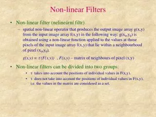
UNIT-2 NON-LINEARWAVE SHAPING
Non-LinearWaveShaping Definition:Theprocesswhereby the form of a signal is changed by transmission through a non-linear network is called Non-linear Wave Shaping. Types: Clippers. Clampers.
ClipperClassifications • Accordingtobiasing,theclippersmaybeclassifiedas • Unbiasedclippersand • Biasedclippers. • Accordingtoconfigurationusedthe clippersmaybe • Seriesdiodeclippers • Parallelorshuntdiodeclippers • Aseries combinationof diode,resistorandreferencesupply • Multi-diodeclippersconsistingofseveraldiodes,resistors • andreferencevoltages • Twoemitter-coupledtransistorsoperatingasanover-driven
Contd… • Accordingtolevelofclippingtheclippersmay be • Positiveclippers • Negativeclippers • Biasedclippersand • Combinationclippers
Clipper • Clippingcircuitsareusedtoremovethepartof a signal that is above or below some defined referencelevel. • Clippersalsoknownas • Voltagelimiters • Current limiters Amplitudeselectors Slicers
Unbiasedclippers(Parallel PositiveClippers) • Withoutthebattery,theoutputof thecircuitbelowwould • bethenegativeportion oftheinputwave(assumingthe • bottomnodeisgrounded). Whenvi>0, thediode ison (short-circuited),viisdropped acrossR andvo=0.Whenvi • <0,thediodeisoff(open-circuited),thevoltageacrossRis • zeroandvo=vi.
Unbiasedclippers(Parallel NegativeClippers) +ive cycle :- anode is at ground potential and cathode sees variable +ive voltage from 0 to +Vm So complete cycle, the diodeisreversebiasedandVo=Vin.AtpositivepeakVo=+5V -ive cycle :- anode is at ground potential and cathode sees variable -ive vols from 0 to –Vm. When magnitude of in put volatgei.e/Vin/>Vd,thediodebecomeforwardbiasedand henceVo=-Vd=0.7V
Seriespositiveclipper +ive cycle :- anode is at ground potential and cathode sees variable+ivevoltagefrom0to+Vm.Forcomlpete,cycle,diode becomereversebiasedandhenceVo=0V -ive cycle :- anode is at ground potential and cathode sees variable -ive voltage from 0 to –Vm. So in complete cycle, the diodeisforwardbiasedandVo=Vin+ Vd andAtnegativepeak, Vo=-Vm+Vd=-5v
SeriesNegativeclipper +ivecycle:-anodeisatpositivepotentialfrom0to +Vm.Forcomlpete, cycle,diodebecomeforwardbiasedandhencevo=5v -ive cycle :- Cathode is at ground potential and cathode sees variable - ive voltage from 0 to –Vm. So in complete cycle, the diode is Reverse biasedandnegativepeak,Vo=0
PositiveShuntclipping withzero referenceRvoltage D Vi Vo V V O O Input Output Transfercharacteristicsequations: Vγ Vγ VO=0forVi>0 VO=ViforVi<0 Slope=1 V [Ideal] i VO=VγforVi>Vγ VO=ViforVi<Vγ D–ON D–OFF V i Input
PositiveShuntclippingwithpositive referencevRoltage D Vi Vo VO VR VO Input Transfer characteristics equations: VR+Vγ VR+VγOutput Vi<VR+Vγ D – OFF Vi VO=Vi Vi>VR+Vγ VO=VR+Vγ D–ON
PositiveShuntclippingwithnegative referencevoltage R D VR VO VO Vo Vi Input Vi Transfer characteristics equation: V i Output Vi Vi>Vγ-VR D–ON VO = Vγ -VR Vi<Vγ-VR VO=Vi D – OFF
NegativeShuntclippingwithzero referencevoltage R VO VO D Vi Vo Input -Vγ -Vγ Transfer characteristic equations: Vi Output Vi Vi>-Vγ D–OFF VO=Vγ Vi< -Vγ D–ON VO=-Vγ
NegativeShuntclippingwithpositive referencevoltage R VO DOFF DON D VR VO Vo Vi Transfer characteristics equations: Vi VR-Vγ Vi<VR-Vγ VO=VR-Vγ Vi D–ON Vi>VR-Vγ D – OFF VO=Vi
NegativeShuntclippingwithnegative referencevoltage R V VO O D Vo Vi V R Vi Transfer characteristic equations: -(Vγ+VR Input Vi<-(Vγ+VR) =-(Vγ+VR) Vi D– ON VO Vi<-(Vγ+VR)D–OFF VO=Vi