Advancements in THz Transistor Electronics: Capabilities and Design Challenges
310 likes | 444 Vues
This paper presents an overview of the current and projected capabilities of THz transistor electronics. It discusses the significance of THz transistors in enabling high-speed digital logic and advanced communication systems, as well as the technical challenges involved in their design, such as thermal resistance, scaling laws, and the impact of fringing capacitance. Key findings include improvements in bandwidth, strategies for high-density designs, and new fabrication processes. Insights are provided into THz Field-Effect Transistors and their scaling challenges, offering a roadmap for future developments.

Advancements in THz Transistor Electronics: Capabilities and Design Challenges
E N D
Presentation Transcript
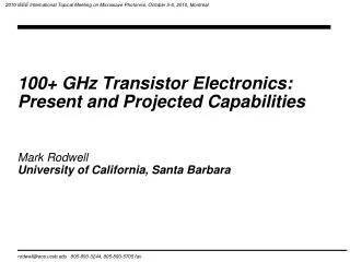
2010 IEEE International Topical Meeting on Microwave Photonics, October 5-6, 2010, Montreal 100+ GHz Transistor Electronics: Present and Projected Capabilities Mark Rodwell University of California, Santa Barbara rodwell@ece.ucsb.edu 805-893-3244, 805-893-5705 fax
Why Build THz Transistors ? 500 GHz digital logic→ fiber optics THz amplifiers→ THz radios→ imaging, sensing, communications precision analog design at microwave frequencies→ high-performance receivers Higher-Resolution Microwave ADCs, DACs, DDSs
Transistor figures of Merit / Cutoff Frequencies H21=short-circuit current gain MAG = maximum available power gain:impedance-matched fmaxpower-gaincutoff frequency gains, dB U= unilateral power gain:feedback nulled, impedance-matched ftcurrent-gaincutoff frequency
What Determines Digital Gate Delay ? → CV/I terms dominate analog ICs have somewhat similar bandwidth considerations...
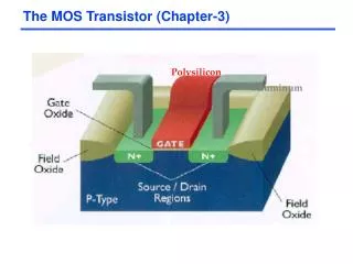
High-Speed Transistor Design Depletion Layers Thermal Resistance Bulk and Contact Resistances Fringing Capacitances
Frequency Limitsand Scaling Laws of (most) Electron Devices PIN photodiode To double bandwidth, reduce thicknesses 2:1 Improve contacts 4:1 reduce width 4:1, keep constant length increase current density 4:1
Changes required to double transistor bandwidth nearly constant junction temperature → linewidths vary as (1 / bandwidth)2 fringing capacitance does not scale → linewidths scale as (1 / bandwidth ) constant voltage, constant velocity scaling
Thermal Resistance Scaling : Transistor, Substrate, Package Probable best solution: Thermal Vias ~500 nm below InP subcollector ...over full active IC area.
150 nm thick collector 256 nm InP HBT Z. Griffith 340 GHz dynamic frequency divider M. Seo, UCSB/TSC 340 GHz VCO 70 nm thick collector M. Seo, UCSB/TSCIMS 2010 E. Lind 324 GHz amplifier J. Hacker, TSCIMS 2010 204 GHz staticfrequency divider Z. Griffith Z. Griffith, TSCCSIC 2010:to be presented much better results in press ...
InP Bipolar Transistor Scaling Roadmap emitter 512 256 128 64 32 nm width16 8 4 2 1 m2 access r base 300 175 120 60 30 nm contact width, 20 10 5 2.5 1.25 m2 contact r collector 150 106 75 53 37.5 nm thick, 4.5 9 18 36 72 mA/m2 current density 4.9 4 3.3 2.75 2-2.5 V, breakdown ft 370 520 730 1000 1400 GHz fmax 490 850 1300 2000 2800 GHz power amplifiers 245 430 660 1000 1400 GHz digital 2:1 divider 150 240 330 480 660 GHz
Chart 17 Initial Results: Refractory-Contact HBT Process 110 nm emitter width 270 nm emitter width Need to add E-beam defined base, best base contact technology
InP DHBTs: August 2010 200 nm 250 nm 110 nm 250 nm 600nm 350 nm
670 GHz Transceiver Simulations in 128 nm InP HBT transmitter exciter Simulations @ 670 GHz (128 nm HBT) LNA: 9.5 dB Fmin at 670 GHz PA: 9.1 dBm Pout at 670 GHz receiver VCO:-50 dBc (1 Hz) @ 100 Hz offsetat 620 GHz (phase 1) 3-layer thin-film THz interconnects thick-substrate--> high-Q TMIC thin -> high-density digital Dynamic divider:novel design,simulates to 950 GHz Mixer: 10.4 dB noise figure11.9 dB gain
THz Field-Effect Transistors (THz HEMTs)
FET Scaling Laws Changes required to double device / circuit bandwidth. laws in constant-voltage limit:
HEMT/MOSFET Scaling: Four Major Challenges gate dielectric:need thinner barriers→ tunneling leakage contact regions:need reduced access resistivity channel:need thinner layers channel:need higher charge densityyet keep high carrier velocity
THz FET Scaling Roadmap ? source-coupled logic @ 200 mV overdrive source / drain regrowth G-L transport high-K gate dielectrics
III-V MOSFETs with Source/Drain Regrowth 27 nm InGaAs MOSFET
Clock Timing Jitter in ADCs and DACs Timing jitter is quantitatively specified by the single-sideband phase noise spectral density L(f). IC oscillator phase noise varies as ~1/f2 or ~1/f3 near carrier Impact on ADCs and DACs: imposition of 1/fn sidebands on signal of relative amplitude L(f) ...not creation of a broadband noise floor. Dynamic range of electronic DACs & ADCs is limited by factors other than the phase noise of the sampling clock
Why ADC Resolution Decreases With Sample Rate Dynamic Range Determined by Circuit Settling Time vs. Clock Period dynamic hysteresis metastability IC time constants→ Resolution decreases at high sample rates
Fast IC Waveform Generation: General Prospects Waveform generator → fast digital memory & DAC Parallel digital memory and 200 Gb/s MUX is feasible cost limits: power & system complexity vs. # bits, GS/s Performance limit: speed vs. resolution of DAC faster technologies → increased sample rates Feasible ADC resolution: 12 SNR bits @ 4 GS/s feasible using 500 nm (400GHz) InP HBT. Feasible sample rate will scale with technology speed..
Few-THz Transistors Few-THz InP Bipolar Transistors: can it be done ? Scaling limits: contact resistivities, device and IC thermal resistances. 62 nm (1 THz ft , 1.5 THz fmax ) scaling generation is feasible. 700 GHz amplifiers, 450 GHz digital logic Is the 32 nm (1 THz amplifiers) generation feasible ? Few-THz InP Field-Effect Transistors: can it be done? challenges are gate barrier, vertical scaling,source/drain access resistance, channel density of states. 2DEG carrier concentrations must increase. S/D regrowth offers a path to lower access resistance. Solutions needed for gate barrier: possibly high-k (MOSFET) Implications: 1 THz radio ICs, ~200-400 GHz digital ICs, 20 GHz ADCs/DACs