Current Status of HCC Device Development and Challenges in Size and Cost Management
The HCC device design has evolved significantly, with the original size expected at 3.5mm x 3.5mm (area ~12.25mm²). However, with 117 bond pads now included, the requirements have changed, impacting overall cost and chip dimensions. The dual-sided pad duplication, driven by hybrid constraints, complicates real estate usage and increases costs. Recent modifications have centered power connections at the device bottom, and further iterations are being pursued to finalize the pad ring design. Although progress is evident, unknowns remain regarding capacitor values and hybrid geometry compatibility.

Current Status of HCC Device Development and Challenges in Size and Cost Management
E N D
Presentation Transcript
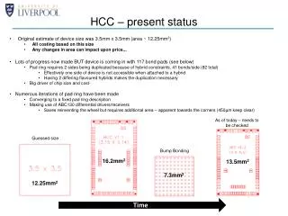
HCC – present status • Original estimate of device size was 3.5mm x 3.5mm (area ~ 12.25mm2) • All costing based on this size • Any changes in area can impact upon price... • Lots of progress now made BUT device is coming in with 117 bond pads (see below) • Pad ring requires 2 sides being duplicated because of hybrid constraints, 41 bonds/side (82 total) • Effectively one side of device is not accessible when attached to a hybrid • Having 2 differing flavoured hybrids makes the duplication necessary • Big driver of chip size and cost- • Numerous iterations of pad ring have been made • Converging to a fixed pad ring description • Making use of ABC130 differential drivers/receivers • Saves reinventing the wheel but requires additional area – apparent towards the corners (450µm keep clear) As of today – needs to be checked Guessed size Bump Bonding 16.2mm2 13.5mm2 7.3mm2 12.25mm2 Time
HCC – present status • As of today • Moved bond pads around whilst trying to maintain minimal duplication • Biggest change is powering now brought in towards the bottom of the device and not the sides • Rest remains more or less the same • Still lots of unknowns • Use of different value capacitors makes it difficult in real estate usage on hybrid • Better to converge to a singe value of capacitance (using arrays) • Array footprint is much smaller – original reason for power pads placed on side decoupled with a single array • Otherwise have to make use of 0402s and 2 x capacitor array Hybrid Data Chip area ~ 13.5mm2 (10% oversize compared to original) Stave TTC ABC130 TTC ABC130 TTC Auxiliary Connections Auxiliary Connections Power Block ABC130 Data ABC130 Data ABC130 Data ABC130 Data
HCC – present status Does it fit on a hybrid? Appears to with no change to hybrid geometry ABC130 TTC Bus yet to be routed PLL and Bandgap Decoupling Power Supply decoupling (100nF and 1µF)
HCC – present status • Alternative, more aggressive proposal, courtesy of Nandor/(Mitch) at Penn • Makes use of dual row bonding throughout • Device size comes in at 3mm x 3mm – though will probably increase.