Transistors
Transistors. ME4447 Spring 2006 Kirk Glazer Joel Schuetz Andrew Timm. Lecture Overview. What is a Transistor? History Types Characteristics Applications. Semiconductors: ability to change from conductor to insulator Can either allow current or prohibit current to flow

Transistors
E N D
Presentation Transcript
Transistors ME4447 Spring 2006 Kirk Glazer Joel Schuetz Andrew Timm
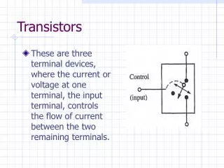
Lecture Overview • What is a Transistor? • History • Types • Characteristics • Applications
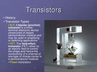
Semiconductors: ability to change from conductor to insulator Can either allow current or prohibit current to flow Useful as a switch, but also as an amplifier Essential part of many technological advances What is a Transistor?
A Brief History • Guglielmo Marconi invents radio in 1895 • Problem: For long distance travel, signal must be amplified • Lee De Forest improves on Fleming’s original vacuum tube to amplify signals • Made use of third electrode • Too bulky for most applications
Bell Labs (1947): Bardeen, Brattain, and Shockley Originally made of germanium Current transistors made of doped silicon The Transistor is Born
How Transistors Work • Doping: adding small amounts of other elements to create additional protons or electrons • P-Type: dopants lack a fourth valence electron (Boron, Aluminum) • N-Type: dopants have an additional (5th) valence electron (Phosphorus, Arsenic) • Importance: Current only flows from P to N
Diode: simple P-N junction. Forward Bias: allows current to flow from P to N. Reverse Bias: no current allowed to flow from N to P. Breakdown Voltage: sufficient N to P voltage of a Zener Diode will allow for current to flow in this direction. Diodes and Bias
npn bipolar junction transistor pnp bipolar junction transistor Bipolar Junction Transistor (BJT) • 3 adjacent regions of doped Si (each connected to a lead): • Base. (thin layer,less doped). • Collector. • Emitter. • 2 types of BJT: • npn. • pnp. • Most common: npn (focus on it). Developed by Shockley (1949)
BJT npn Transistor • 1 thin layer of p-type, sandwiched between 2 layers of n-type. • N-type of emitter: more heavily doped than collector. • With VC>VB>VE: • Base-Emitter junction forward biased, Base-Collectorreverse biased. • Electrons diffuse from Emitter to Base (from n to p). • There’s a depletion layer on the Base-Collector junction no flow of e- allowed. • BUT the Base is thin and Emitter region is n+ (heavily doped) electrons have enough momentum to cross the Base into the Collector. • The small base current IB controls a large current IC
BJT characteristics • Current Gain: • α is the fraction of electrons that diffuse across the narrow Base region • 1- α is the fraction of electrons that recombine with holes in the Base region to create base current • The current Gain is expressed in terms of the β (beta) of the transistor (often called hfe by manufacturers). • β (beta) is Temperature and Voltage dependent. • It can vary a lot among transistors (common values for signal BJT: 20 - 200).
npn Common Emitter circuit • Emitter is grounded. • Base-Emitter starts to conduct with VBE=0.6V,IC flows and it’s IC=b*IB. • Increasing IB, VBE slowly increases to 0.7V but IC rises exponentially. • As IC rises ,voltage drop across RC increases and VCE drops toward ground. (transistor in saturation, no more linear relation between IC and IB)
Common Emitter characteristics Collector current controlled by the collector circuit. (Switch behavior) In full saturation VCE=0.2V. Collector current proportional to Base current The avalanche multiplication of current through collector junction occurs: to be avoided No current flows
BJT as Switch • Vin(Low ) < 0.7 V • BE junction not forward biased • Cutoff region • No current flows • Vout = VCE = Vcc • Vout = High • Vin(High) • BE junction forward biased (VBE=0.7V) • Saturation region • VCE small (~0.2 V for saturated BJT) • Vout = small • IB = (Vin-VB)/RB • Vout = Low
BJT as Switch 2 • Basis of digital logic circuits • Input to transistor gate can be analog or digital • Building blocks for TTL – Transistor Transistor Logic • Guidelines for designing a transistor switch: • VC>VB>VE • VBE= 0.7 V • IC independent from IB (in saturation). • Min. IB estimated from by (IBmin» IC/b). • Input resistance such that IB > 5-10 times IBminbecause b varies among components, with temperature and voltage and RB may change when current flows. • Calculate the max IC and IB not to overcome device specifications.
BJT as Amplifier • Common emitter mode • Linear Active Region • Significant current Gain • Example: • Let Gain, b = 100 • Assume to be in active region -> VBE=0.7V • Find if it’s in active region
BJT as Amplifier VCB>0 so the BJT is in active region
Field Effect Transistors • Similar to the BJT: • Three terminals, • Control the output current • In 1925, the fundamental principle of FET transistors was establish by Lilienfield. • 1955 : the first Field effect transistor works • Increasingly important in mechatronics.
Field Effect Transistors • Three Types of Field Effect Transistors • MOSFET (metal-oxide-semiconductor field-effect transistors) • JFET (Junction Field-effect transistors) • MESFET (metal-semiconductor field-effect transistors) • Two Modes of FETs • Enhancement mode • Depletion mode • The more used one is the n-channel enhancement mode MOSFET, also called NMOS
FET Architecture • Enhanced MOSFET • Depleted MOSFET • JFET Nonconducting Region Conducting Region Nonconducting Region
NMOS Voltage Characteristic • VDS = Constant • VGS > Vth : • 0 < VDS < VPinch off • Active Region • IDS controlled by VGS VGS < Vth IDS=0 • VDS > VPinch off • Saturation Region • IDS constant Active Region Saturation Region • VDS > VBreakdown • IDS approaches IDSShort • Should be avoided VPinchoff
NMOS uses • High-current voltage-controlled switches • Analog switches • Drive DC and stepper motor • Current sources • Chips and Microprocessors • CMOS: Complementary fabrication
The circuit symbols: JFET design: JFET overview
Junction Field Effect Transistor Difference from NMOS • VGS > Vth IDS=0 • VGS< -Vth : • 0 < VDS < VPinch off • Active Region • IDS controlled by VGS Saturation Region Active Region • VDS > VPinch off • Saturation Region • IDS constant • VDS > VBreakdown • IDS approaches IDSShort • Should be avoided VPinchoff
JFET uses • Small Signal Amplifier • Voltage Controlled Resistor • Switch
FET Summary • General: • Signal Amplifiers • Switches • JFET: • For Small signals • Low noise signals • Behind a high impedence system • Inside a good Op-Ampl. • MOSFET: • Quick • Voltage Controlled Resistors • RDS can be really low : 10 mOhms
Power Transistors • In General • Fabrication is different in order to: • Dissipate more heat • Avoid breakdown • So Lower gain than signal transistors • BJT • essentially the same as a signal level BJT • Power BJT cannot be driven directly by HC11 • MOSFET • base (flyback) diode • Large current requirements
Various Types of Transistors • TempFET – MOSFET’s with temperature sensor • High Electron Mobility Transistors (HEMTs) – allows high gain at very high frequencies • Darlington – two transistors within the same device, gain is the product of the two inidvidual transistors
Shockley Diode/Thyristor • Four-layer PNPN semiconductor devices • Behaves as two transistors in series • Once on, tends to stay on • Once off, tends to stay off
TRIAC • Triode alternating current switch • Essentially a bidirectional thyristor • Used in AC applications • Con: Requires high current to turn on • Example uses: Modern dimmer switch
References • www.lucent.com • http://transistors.globalspec.com • http://www.kpsec.freeuk.com • www.Howstuffworks.com • www.allaboutcircuits.com • Previous student lectures