Multicycle Approach
Multicycle Approach. Break up the instructions into steps each step takes one clock cycle balance the amount of work to be done in each step/cycle so that they are about equal restrict each cycle to use at most once each major functional unit so that such units do not have to be replicated


Multicycle Approach
E N D
Presentation Transcript
Multicycle Approach • Break up the instructions into steps • each step takes one clock cycle • balance the amount of work to be done in each step/cycle so that they are about equal • restrict each cycle to use at most once each major functional unit so that such units do not have to be replicated • functional units can be shared between different cycles within one instruction • Between steps/cycles • At the end of one cycle store data to be used in later cycles of thesame instruction • need to introduce additional internal (programmer-invisible) registers for this purpose • Data to be used in later instructions are stored in programmer-visible state elements: the register file, PC, memory
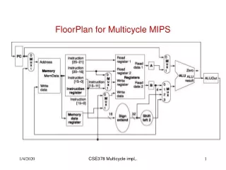
Multicycle Approach • Note particularities of multicyle vs. single- diagrams • single memory for data and instructions • single ALU, no extra adders • extra registers to hold data between clock cycles Single-cycle datapath Multicycle datapath (high-level view)
Multicycle Datapath Basic multicycle MIPS datapath handles R-type instructions and load/stores: new internal register in red ovals, new multiplexors in blue ovals
Breaking instructions into steps • Our goal is to break up the instructions into steps so that • each step takes one clock cycle • the amount of work to be done in each step/cycle is about equal • each cycle uses at most once each major functional unit so that such units do not have to be replicated • functional units can be shared between different cycles within one instruction • Data at end of one cycle to be used in next must be stored !!
Breaking instructions into steps • We break instructions into the following potential execution steps – not all instructions require all the steps – each step takes one clock cycle • Instruction fetch and PC increment (IF) • Instruction decode and register fetch (ID) • Execution, memory address computation, or branch completion (EX) • Memory access or R-type instruction completion (MEM) • Memory read completion (WB) • Each MIPS instruction takes from 3 – 5 cycles (steps)
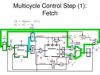
Step 1: Instruction Fetch & PC Increment (IF) • Use PC to get instruction and put it in the instruction register. Increment the PC by 4 and put the result back in the PC. • Can be described succinctly using RTL (Register-Transfer Language): IR = Memory[PC]; PC = PC + 4; IR = Instruction Register
Step 2: Instruction Decode and Register Fetch (ID) • Read registers rs and rt in case we need them. Compute the branch address in case the instruction is a branch. • RTL:A = Reg[IR[25-21]];B = Reg[IR[20-16]];ALUOut = PC + (sign-extend(IR[15-0]) << 2);
Step 3: Execution, Address Computation or Branch Completion (EX) • ALU performs one of four functions depending on instruction type • memory reference:ALUOut = A + sign-extend(IR[15-0]); • R-type:ALUOut = A op B; • branch (instruction completes):if (A==B) PC = ALUOut; • jump (instruction completes): PC = PC[31-28] || (IR(25-0) << 2)
Step 4: Memory access or R-type Instruction Completion(MEM) • Again depending on instruction type: • Loads and stores access memory • load MDR = Memory[ALUOut]; • store (instruction completes) Memory[ALUOut] = B; • R-type (instructions completes)Reg[IR[15-11]] = ALUOut; MDR = Memory Data Register
Step 5: Memory Read Completion (WB) • Again depending on instruction type: • Load writes back (instruction completes) Reg[IR[20-16]]= MDR; Important: There is no reason from a datapath (or control) point of view that Step 5 cannot be eliminated by performing Reg[IR[20-16]]= Memory[ALUOut]; for loads in Step 4. This would eliminate the MDR as well. The reason this is not done is that, to keep steps balanced in length, the design restriction is to allow each step to contain at most one ALU operation, or one register access, or one memory access.
Summary of Instruction Execution Step 1: IF 2: ID 3: EX 4: MEM 5: WB
4 Multicycle Execution Step (1):Instruction Fetch IR = Memory[PC]; PC = PC + 4; IR = Instruction Register MDR = Memory Data Register PC + 4 Must be MUX
Reg[rs] PC + 4 Reg[rt] Multicycle Execution Step (2):Instruction Decode & Register Fetch A = Reg[IR[25-21]]; (A = Reg[rs]) B = Reg[IR[20-15]]; (B = Reg[rt]) ALUOut = (PC + sign-extend(IR[15-0]) << 2) * Branch Target Address *
Reg[rs] Mem. Address PC + 4 Reg[rt] Multicycle Execution Step (3):Memory Reference Instructions ALUOut = A + sign-extend(IR[15-0]);
Reg[rs] R-Type Result PC + 4 Reg[rt] Multicycle Execution Step (3):ALU Instruction (R-Type) ALUOut = A op B
Branch Target Address Reg[rs] Reg[rt] Multicycle Execution Step (3):Branch Instructions if (A == B) PC = ALUOut; Branch Target Address
Branch Target Address Reg[rs] Reg[rt] Multicycle Execution Step (3):Jump Instruction PC = PC[31-28] concat (IR[25-0] << 2) Jump Address
Mem. Address Reg[rs] PC + 4 Reg[rt] Multicycle Execution Step (4):Memory Access - Read (lw) MDR = Memory[ALUOut]; Mem. Data
Reg[rs] PC + 4 Reg[rt] Multicycle Execution Step (4):Memory Access - Write (sw) Memory[ALUOut] = B;
Reg[rs] R-Type Result PC + 4 Reg[rt] Multicycle Execution Step (4):ALU Instruction (R-Type) Reg[IR[15:11]] = ALUOUT
Reg[rs] Mem. Address PC + 4 Mem. Data Reg[rt] Multicycle Execution Step (5):Memory Read Completion (lw) Reg[IR[20-16]] = MDR;
Multicycle Datapath with Control I … with control lines and the ALU control block added – not all control lines are shown
Multicycle Datapath with Control II New gates New multiplexor For the jump address Complete multicycle MIPS datapath (with branch and jump capability) and showing the main control block and all control lines
Multicycle Control Step (1):Fetch IR = Memory[PC]; PC = PC + 4; 1 1 0 0 0 X 010 0 X 1 0 1
Multicycle Control Step (2):Instruction Decode & Register Fetch A = Reg[IR[25-21]]; (A = Reg[rs]) B = Reg[IR[20-15]]; (B = Reg[rt]) ALUOut = (PC + sign-extend(IR[15-0]) << 2); 0 0 X 0 0 X 010 X X 0 0 3
Multicycle Control Step (3):Memory Reference Instructions ALUOut = A + sign-extend(IR[15-0]); 0 0 X 1 0 X 010 X X 0 0 2
Multicycle Control Step (3):ALU Instruction (R-Type) ALUOut = A op B; 0 0 X 1 0 X ??? X X 0 0 0
Multicycle Control Step (3):Branch Instructions if (A == B) PC = ALUOut; 0 1 if Zero=1 X 1 0 X 011 1 X 0 0 0
Multicycle Execution Step (3):Jump Instruction PC = PC[21-28] concat (IR[25-0] << 2); 0 1 X X 0 X XXX 2 X 0 0 X
Multicycle Control Step (4):Memory Access - Read (lw) MDR = Memory[ALUOut]; 0 0 1 X 0 X XXX X X 1 0 X
Multicycle Execution Steps (4)Memory Access - Write (sw) Memory[ALUOut] = B; 0 0 1 X 1 X XXX X X 0 0 X
2 0 1 M MUX 1 U X 0 0 M 0 M U U 1 X 1 0 X M U 1 X 0 1 M U 2 X 3 E X T N D Multicycle Control Step (4):ALU Instruction (R-Type) Reg[IR[15:11]] = ALUOut; (Reg[Rd] = ALUOut) 0 IRWrite I 28 32 0 I Instruction jmpaddr R <<2 CONCAT I[25:0] 5 PCWr* rs rt rd X X RegDst 0 32 5 5 1 XXX IorD ALUSrcA 5 PC Operation RN1 RN2 WN 3 MemWrite M ADDR PCSource Registers Zero D A X RD1 Memory ALU WD R RD ALU OUT B WD RD2 4 MemRead MemtoReg 1 RegWrite 0 1 ALUSrcB 16 32 immediate X <<2
2 0 1 M MUX 1 U X 0 0 M 0 M U U 1 X 1 0 X M U 1 X 0 1 M U 2 X 3 E X T N D Multicycle Execution Steps (5)Memory Read Completion (lw) Reg[IR[20-16]] = MDR; 0 IRWrite I 0 28 32 I Instruction jmpaddr R <<2 CONCAT I[25:0] 5 PCWr* rs rt rd X X 0 RegDst 32 0 XXX 5 5 IorD ALUSrcA 5 PC Operation RN1 RN2 WN 3 MemWrite M ADDR PCSource Registers X Zero D A RD1 Memory ALU WD R RD ALU OUT B WD RD2 4 MemRead MemtoReg 0 0 RegWrite 1 ALUSrcB X 16 32 immediate <<2