Download
1 / 39
400 likes | 460 Vues
Gain insights into analog-to-digital conversion methods such as successive approximation and flash converters. Explore the impact of errors in ADC and the use of DACs in various applications. Learn about dual-slope conversion, counting converters, sample-and-hold circuits, and more. Discover key concepts like resolution, step size, and range in ADC operations.

E N D
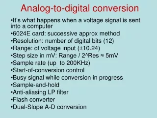
Analog-to-digital conversion It’s what happens when a voltage signal is sent into a computer 6024E card: successive approx method Resolution: number of digital bits (12) Range: of voltage input (±10.24) Step size in mV: Range / 2^Res ≈ 5mV Sample rate (up to 200KHz) Start-of-conversion control Busy signal while conversion in progress Sample-and-hold Anti-aliasing LP filter Flash converter Dual-Slope A-D conversion
ADC methods Flash converter: use of analog comparators Errors in ADC… (time-out for DAC details): Power-of-2 source resistors vs R-2R ladder analog switches for digital inputs reference voltage for HI; gnd for LO multiplying DAC Bipolar DAC ADA lab: 7524 + 353 Counting converter—variable sample rate Successive approximation Dual slope
TRUTH TABLE for converting X Y Z to binary numbers X Y Z B A 0 0 0 0 0 0 0 1 0 1 0 1 1 1 0 1 1 1 1 1 • What should B be? Y! • What about A? X xor Y xor Z will work, as will Z and X xnor Y • To make an N-bit flash conversion we need 2^N - 1 comparators. • For an 8-bit conversion 255 comparators are required! • A costly proposition, but necessary where blinding speed is required (in radar, for example). • Try the AD9002-B 8-bit flash converter, with 160 MHz bandwidth, 750 mW power consumption and a cost of $200 per chip • Or the 6-bit, 200 MHz, AD9006, at $320 per chip, for use in digital oscilloscopes. • year 2000 prices…
Errors in ADC Thanks to rejiggering resistors, error is now ±½LSB
nerve cell as digital to analog convertermany inputs, one output…
Review of neg. gain summ. amp: Extend this idea to N inputs, with each Rsn = 2*Rs(n-1)where Rs1 is the MSB
Analog switches in the service of a multiplying3-bit D-A converter would look like: allow Vref to be variable for multiplication…
Bipolar DAC with R-2R ladder: Should be -5v… The R-2R ladder uses twice as many resistors, but of only 2 sizes… When the digital input is 0 0 0 0 the offset output is +1.25 volts If logical 1 = Vref, then the max output above is = -(15/16)*Vref An R-2R ladder is in the 7524 DAC chip for Lab ADA…
Settling time. Consider a 4-bit DAC that must change from 7 to 8, due to input change of 0111 to 1000. All the input bits are switching at once. If the analog switches in the DAC bits change slower from LO to HI than HI to LO, then there will be a brief pause when the DAC output drops to 0 before jumping up to 8.
7533 features • Low cost 10-bit DAC • Low cost AD7524 replacement • Linearity: ½ LSB, 1 LSB, or 2 LSB • Low power dissipation • Full 4-quadrant multiplying DAC • CMOS/TTL direct interface • Latch free (protection Schottky not required) • Endpoint linearity • http://www.analog.com/static/imported-files/data_sheets/AD7533.pdfsee for circuit diagram with op amp...
DAC step size should say “step size” instead of resolution… An 8-bit resolution for 5.12 v range results in 40mV step size
Using all the bits you can If your signal is so small as to cover only a few steps your output will look like a miniature staircase…You need more gain! … could decrease Vref, also…
Learning to be a DAC (Hebb’s Law)more later in lecture on adaptive gain control • work\fold23\D2A_learn_2010 for jj = 1:4 % update each weight delW = err_now*trn_set_col( jj )*mew; % Hebb's rule W_col(jj) = W_col(jj) + delW; end Learn Grey code to avoid transient glitches?: one bit changes per clock pulse…
Action of counting converter • Connect an up-counter's outputs to a DAC's digital inputs, making sure to hook up the counter's MSB to the DAC's MSB, and so on. • Connect output of the DAC to the V+ side of an analog comparator like the LM311. • Connect the unknown Analog input = AIN to the V- side of the comparator. • Start by CLEARing the counter to 0000. Send pulses into its clock. • With each count up the DAC output will increase by a step. • At some point DAC-out will become greater than analog-in, and will send the output of the comparator from LO to HI. • When the comparator output switches from 0 to 1, have it hold the count. • The output of the counter at the time it's “held” is the answer! (memory) • The answer is a 4-bit digital code which represents analog-in • If the comparator output is LO then this ADC is BUSY.
Problems with counting converter • What if Ain is greater than DAC output MAX for 1111 = input? • The sampling rate is not constant (smaller Ain’s convert faster than larger) • It takes 16 clock pulses to convert the largest Ain. • Ain can’t change while (long) conversion is occurring
digression: sample & hold • Capacitor holds the sampled signal: only high-Z paths for cap to discharge • The smaller the capacitor (pico farad?), the faster it will charge up: want low Z output resistance from the left, through FET switch. • Cap can “droop” during hold by leaking through op amp +input • FET switch is low Z for pos. sample pulse • sample pulse should occur just before A-D conversion begins
Improvements of SA over counting converter • No problem converting Ain > DACmax to 1111 • N clock pulses needed for N bit conversion: Example: for 8 bits counting converter might need 256 clock pulses, SA will need 8 clock cycles always • Sample rate is constant • SA plays “20 questions” with unknown Ain: decreases range of unknown by factor of 2 on each cycle. • EOC = end of conversion signal is HI on last bit ofone-hot sequencer. (EOC must latch answer) • Can operate normally in a continuous re-sample mode
Dual Slope A-D conversion • integrating A-D converter: no need for sample and hold • found in digital multimeters • utilizes current-voltage relationship of capacitor:
Dual Slope Timing: • May need sign-changing op amp to match with circuit diagram • Longer count time→greater number to be displayed at zero-crossing • No need for sample and hold because signal is “averaged” over conversion time • For DMM conversion cycle time is about 250 msec
Bipolar analog representation:2’s complement code 1 -1 = 0 0 0 1 + 1 1 1 1 0 0 0
Review • Fastest A-D conversion is flash with comparators • D-A conversion with neg gain summation ampand R-2R ladder of resistors • Successive approx for N bits of resolution needs N clock cycles for conversion; final clock cycle is end-of-conversion signal • May need anti-aliasing LP filter and sample & hold on input to A-D converter • Dual slope A-D averages analog-in over long cycle