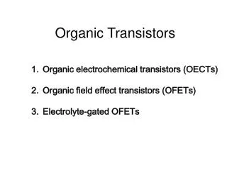
Organic Transistors
Organic Transistors. Organic electrochemical transistors (OECTs) Organic field effect transistors (OFETs) Electrolyte-gated OFETs. 1. Organic Electrochemical Transistors (OECTs). Reversible oxidation and reduction switching

Organic Transistors
E N D
Presentation Transcript
Organic Transistors • Organic electrochemical transistors (OECTs) • Organic field effect transistors (OFETs) • Electrolyte-gated OFETs
1. Organic Electrochemical Transistors (OECTs) • Reversible oxidation and reduction switching • Electrochemical devices uses both electrons and ions as charge carriers reduction PEDOT+PSS- + M+ + e-PEDOT0 + M+PSS- Conducting Semi-conducting Transparent Deep blue colored oxidation
e- e- e- 1.1.The dynamic configuration Structure 1 (one area of conducting polymer) • Reduction at the negatively biased side of electrode • oxidation at the positively biased side of electrode • Dynamic behavior M+ M+ M+ red ox - V +
e- e- 1.2 The bi-stable configuration Structure 2 (two areas of conducting polymer) • Reduction at the negatively biased electrode • Oxidation at the positively biased electrode • Bi-stable behavior red ox PEDOT+PSS- + M+ + e-PEDOT0 + M+PSS- M+ M+ M+ red ox - V +
The first transistor (1947) Size: 2.5cm Flexible substrates A flexible organic electrochemical transistor
Structure 2 VG Structure 1 VD Electrolyte 1.3 The three-terminal transistor Common ground G D S PEDOT:PSS
Potential Absorption Pinch-off • Pinch-off due to the decrease of charge carriers at the drain side of the channel • Almost all resistance is located within 100µm of the channel edge • Effect of structure 1 S+ D- Svensson et al. (2003) POLYTRONIC
Chronoamperometric response • Comparison between lateral and vertical design
Nafion • Cation conductor, mainly protons. • Forms inverted micelle clusters with sulphonic acid groups on the inner surface • The micelles are joined through canals. • Charge transport by cations wandering between –SO3- groups. • Ion conduction increases with water content due to swelling and dissociation of ions. Increase of water content
Humidity sensor • Transducer part: EC-transistor • Sensitive part: Nafion G+ VG Nafion D S VD G-
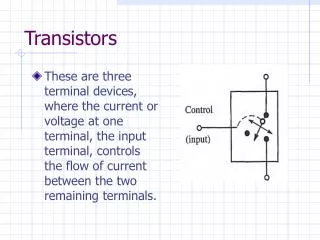
conducting channel semiconductor insulator ID VD 2. Organic Field-Effect Transistors (OFETs) Structure of an Organic Thin Film Transistor + source drain – – – – – – – – – – – – – – – – – – gate - VG By G. Horowitz
2.1. Current-voltage characteristics 2.1.1. Transfer characteristic A FET is basically a capacitor, where one plate is constituted by the gate electrode, and the other one by the semiconductor film. When a voltage Vg is applied between source and gate, majority carriers accumulate at the insulator-semiconductor interface, leading to the formation of a conduction channel between source and drain. ON = conduction channel open The charge in the channel is modulated by adjusting Vg, so that the device behaves as a variable resistance. OFF = No conduction channel A potential signal Vg is transformed in a current signal Id
2.1.2. Current-voltage No analytical solution, unless the mobility is assumed to be constant. If Vd small, the charge is nearly constant over the channel and the drain current is : Linear If Vd > Vg, the channel is pinched-off: Saturation
2.1.3. Output characteristic Linear regime: For a given Vg>0, the current provided by the conduction channel increases with Vd. The drain electrode inject the charge carriers passing through the channel, the channel let pass as many charges the drain electrode injects. Vg controls the doping level N in the conduction channel: large Vg large current Id W and L= channel width and length Ci= capacitance of the insulator layer μ = field-effect mobility VT= threshold voltage (accounts for voltage drops of various origin across the insulator-semiconductor interface) Vg No conduction channel
Output characteristic Saturation regime: For a given Vg, when Vd=Vg, the electrical potential between drain and gate is zero. This destroys the capacitor created between the doped channel and the gate : pinch off. The channel is then interrupted close to the drain. Saturation Vg
2.1.4. How to get the field effect mobility? 1) If Vd small, the charge is nearly constant over the channel and the drain current is : Z=channel width Linear • The channel conductance gd can be expanded to first order: 2) A further step of the method consists of introducing a contact series resistance Rs, which leads to
2.2. Film morphology versus field-effect mobility Potential distribution The mobility measured with a FET is characteristic for the whole film. It is thus expected to depend on the quality of the organic film; especially the quality of the first mono-layers deposited on the insulator
2.2.1. The distribution of charge in the channel (from Poisson’s equation): εs = permittivity of the organic semiconductor q = electron charge Ci= capacitance (per unit area) of the insulator The first molecular layer is important! G. Horowitz, Synthetic Metals 138 (2003) 101–105
The channel reduces to the first monolayer The organic TFT is a 2D device Structural order in the first monolayer is crucial • High mobility along the layers • Monolayer thickness= 1.25 nm for tetracene Dimitrakopoulos, Adv. Mater. 2002, 14, 99
2.2.2. Grain size dependence mobility Polycrystalline film Grain(G) Grain boundary (GB) Length of the GB
Charge transport in polycrystalline media • divide the material into high (crystal grains) and low (grain boundaries) conductivity region. • As grains and grain boundaries are connected in series: Rtot=RG+RGB • R=ρL/S (ρ=resistivity) • for the same surface SG=SGB (active thickness in the FET), we can write ρL= ρGLG+ ρGBLGB • Conductivity σ= 1/ρ÷ pμe if the concentration in charge carrier ”p” is similar in both regions, the effective mobility of the medium is given by
2.3. Mobility and architecture evolution • Organic material can have a mobility larger than amorphous silicon • Saturation with oligoacene maybe with another molecule, mobility will go higher… Mobility for OTFT (at RT)
Discotic liquid crystals A. M. van de Craats et al, Adv. Mater., 2003, 15, 495
Ink-jet Printed OFET’s H. Sirringhaus, Science,290 (2000) Fig. 1. (A) Schematic diagram of high-resolution IJP onto a prepatterned substrate. (B) AFM showing accurate alignment of inkjet-printed PEDOT/PSS source and drain electrodes separated by a repelling polyimide (PI) line with L = 5 µm. (C) Schematic diagram of the top-gate IJP TFT configuration with an F8T2 semiconducting layer (S, source; D, drain; and G, gate). (D) Optical micrograph of an IJP TFT (L = 5 µm). The image was taken under crossed polarizers so that the TFT channel appears bright blue because of the uniaxial monodomain alignment of the F8T2 polymer on top of rubbed polyimide. Unpolarized background illumination is used to make the contrast in the remaining areas visible, where the F8T2 film is in an isotropic multidomain configuration. The arrow indicates pronounced roughness of the unconfined PEDOT boundary.
H. Sirringhaus, Science,290 (2000) A) Transfer characteristics of an IJP TFT with F8T2 aligned uniaxially parallel to the current flow (L = 5 µm, W = 3000 µm) measured under an N2 atmosphere. Subsequent measurements with increasing (solid symbols) and decreasing (open symbols) gate voltage are shown. (B) Scaling of the output characteristics of IJP F8T2 TFTs normalized by multiplying the drain current by the channel length (dashed lines with open symbols, L = 20 µm; solid lines with solid symbols, L = 5 µm). Subsequent measurements with increasing (upward triangles) and decreasing (downward triangles) gate voltage are shown.
3. Electrolyte-gated OFETs The use of a polyelectrolyte allows combining the advantages of the electrochemical transistors (low-voltage <1V, robustness, less sensitive to thickness) and the advantage of the OFETs (fast response < 0.3ms).
Low-cost plastic transistors • 1) For portable applications: compatible with printable batteries (~1.5V) Low voltage • 2) For “one-use” applications: compatible with roll-to-roll printing techniques Robustness, printable electrodes, thicker layers • 3) For logic applications: Fast response, low capacitive currents The Challenge: To combine those properties
Electric double layer capacitors (EDLCs) P(VPA-AA) Proton migration electrode -45° electrode C R polyelectrolyte ~0.1 V Capacitive behavior EDLC builds up at the electrodes Resistive behavior Protons migrate away from the polymer chains 170 kHz (6 μs)
Electric double layer capacitor gated OFETs • Protons migrate to the gate and form an EDLC • Simultaneously, holes injection at Au/P3HT contact and formation of an EDLC at the P3HT-polyanion interface • The channel is open
Transistor characteristics Ti 54 nm P(VPA-AA) RR-P3HT Au Au Au SiO2 Si wafer L = 9 µm, W = 200 µm Extracted mobility: ~0.012 cm2 V-1 s-1
Response Time VD = -1 V; VG = -1 V when 0 s ≤ t ≤ 0.5 s -0 V otherwise Rise: 60% in ~0.1 ms Fall: 90% in <0.3 ms
OFET is OFF S Gate P3HT D Immobile anions Towards the mechanism OFET is ON A. Field-effect vs. Electrochemistry S Gate P3HT H+ D Immobile anions
Electrochemical transistor is ON S ClO4- Gate Li+ D Penetration of anions Towards the mechanism A. Field-effect vs. Electrochemistry VG=0, but not completely OFF S ClO4- Gate D
B. EDLC builds independently of the channel-gate distance Laterally gated OFET Hemispherical PE G 1.1 mm ~0.2 mm G S D S D