Download
1 / 26
410 likes | 970 Vues
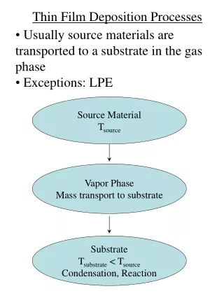
Applications of Chemical Engineering Principles to Thin Film Deposition Process Development. Collin Mui Chemical Engineering 140 Guest Lecture Stanford University May 22, 2008. Thin film deposition processes Chemical vapor deposition Atomic layer deposition Reactor design and applications

E N D
Applications of Chemical Engineering Principles to Thin Film Deposition Process Development Collin Mui Chemical Engineering 140 Guest Lecture Stanford University May 22, 2008
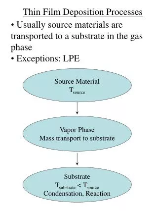
Thin film deposition processes Chemical vapor deposition Atomic layer deposition Reactor design and applications PDL™ Oxide Make sure it works Mechanism of thin film deposition Lesson 1: Chemical kinetics modeling Thin Film Deposition Process Development Silanol TMA Wafer • Make sure it works the same way • Temperature effects on deposition • Lesson 2: Heat transfer • Make sure it works the same way at high yield and low cost • Defect detection and reduction • Lesson 3: Particle transport Fthermo Fdrag Fgrav Novellus Systems Proprietary Information
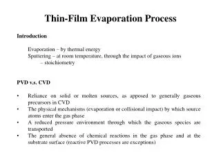
Chemical vapor deposition (CVD) Films deposited by CVD Thin Film Deposition Process and Applications Precursor Desorption Passivation SiO2 Inter Metal Dielectric (IMD) SURFACE REACTION Pre Metal Dielectric (PMD) • Atomic layer deposition (ALD) Shallow Trench Isolation (STI) Deep Trench Isolation Novellus Systems Proprietary Information
Thin Film Deposition Reactor • Novellus™ deposition reactor • Chemical engineering principles Precursor delivery Fluid dynamics Reaction kinetics Temperature control Heat transfer Novellus Systems Proprietary Information
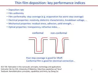
PDL™ Oxide: Enabling technology Conformal insulator layer Thick films (10kÅ) possible Low temperature deposition No plasma damage PDL™ Oxide: Precise engineering Accurate thickness control Excellent repeatability High productivity and manufacturability 3D-Interconnect: Wafer level packaging Insulating oxide liner for through wafer vias (TWVs) Large CD but high AR structures Thickness = 2000 – 10000Å PDL™ Oxide – A Novel Technology • Capacitor sacrificial layer • Sacrificial oxide layer for subsequent etch or CMP • Thickness = 500 - 2000Å • Lithography spacer or oxide liner • Reduce CD limit of lithography • Thin oxide spacer or liner film • Thickness = 50Å to 700Å Novellus Systems Proprietary Information
Catalytic Monolayer Catalytic Monolayer AR ~ 4.5 AR ~ 8 Surface Polymerization AR ~ 17 Catalytic Monolayer Silica Surface Polymerization Catalytic Monolayer Surface Polymerization Conformal Film Deposition via Surface Reactions Trench fill mechanism extendable to high aspect ratio structures Novellus Systems Proprietary Information
PDL Module 300 mm Handler (WTS) PDL Process Module Architecture and Productivity • PDL™ process module • Novellus™ Multi-Station Sequential Deposition (MSSD) architecture • Processes 4 wafers at the same time Silanol Station • Separation of half reactions • Each station performs a half reaction • Improves defect performance Catalyst Station • Precursor delivery system • Accurate and repeatable thickness control • Tunable thickness with good uniformity • Scalable from thin to thick films Novel architecture results in high productivity and accurate control Novellus Systems Proprietary Information
Silanol TMA Wafer Wafer Wafer Nucleation Surface reactions only Self-limiting process Chain Insertion Sequential deposition High deposition rate Cross-Linking Diffusion limited growth Conformal gap fill Surface Chemistry of the PDL Process • Sequential trimethylaluminum (TMA) and silanol exposure • One monolayer of TMA catalyzes multiple silanol insertions • Cross-linking and diffusion lead to self-limiting deposition Novellus Systems Proprietary Information
Silanol TMA Wafer Wafer Wafer Chain Insertion Nucleation Cross-Linking Silanol Film Chain R F C Lesson 1 – Chemical Engineering Kinetics The process can be modeled as a “consecutive reaction” Novellus Systems Proprietary Information
Consecutive reaction Time-dependent concentration 1.0 0.9 R F 0.8 0.7 0.6 Concentration 0.5 0.4 C 0.3 0.2 0.1 0.0 0 1 2 3 4 5 6 7 8 9 10 Time 1.0 0.9 0.8 0.7 Temp 0.6 Concentration 0.5 0.4 0.3 0.2 0.1 0.0 0 5 10 15 20 25 30 35 40 45 50 Time Kinetic Modeling of Consecutive Reactions • Kinetic equations • Temperature dependence • Solution of differential equations Novellus Systems Proprietary Information
Process space for thickness control Deposition temperature Precursor delivery Deposition time Tunable film properties Tunable film stress Tunable wet etch rate Kinetics at different temperatures WERR (100:1 HF) Thermal Oxide 14.0 13.0 12.0 11.0 Wet Etch Rate Ratio 10.0 9.0 8.0 7.0 6.0 60 80 100 120 140 160 180 200 220 Temperature (°C) WERR (100:1 HF) ~150A/cyc (Thermal Oxide) WERR (100:1 HF) ~250A/cyc (Thermal Oxide) Tuning Film Properties by Deposition Temperature Deposition at low temperature Deposition at high temperature Deposition at low temperature Deposition at high temperature Novellus Systems Proprietary Information
Importance of temperature control Inadequate heating 200 180 160 140 120 Wafer Temperature (C) 100 80 60 40 20 0 0 30 60 90 120 150 180 Time (s) 200 180 160 140 120 Wafer Temperature (C) 100 80 60 40 20 0 0 30 60 90 120 150 180 Time (s) Lesson 2 – Wafer Heating and Heat Transfer Cycle 1 Cycle 2 Cycle 3 • Adequate heating Temperature control Heat transfer Cycle 1 Cycle 2 Cycle 3 Stable Temperature = Stable Process Novellus Systems Proprietary Information
Heat Transfer Mechanisms Convection Conduction Radiation T1 T1 1,T1 x1 u k x2 T2 T2 2,T2 Gas velocity Gas pressure Thermal conductivity Pedestal-wafer gap Temperature Emissivity Novellus Systems Proprietary Information
LPCVD Reactor Pressure = 10 mT to 10 T Gas = N2 Final temperature = 200 °C Flow = variable Effect of gas flow rate on convective heat transfer For typical CVD reactors, flow rate ~ 100 to 5000 sccm Insignificant heat transfer by convection Less than 10% of the heat is transferred by convection Usually ignore convection in calculating wafer heating rate Heat Transfer by Convection T1 u T2 Usually ignore convection in calculating wafer heating rate Novellus Systems Proprietary Information
LPCVD Reactor Flow = 100 sccm to 10 slm Gas = N2 Final temperature = 200 °C Pressure = variable Effect of gas pressure on conductive heat transfer LPCVD ~ 10 mT to 1 T APCVD ~ 100 T Conduction is the major heat transfer mechanism Mean free path of gas is short at low pressures While pressure does not affect thermal conductivity, the “effective pedestal-wafer gap” is reduced at low pressures Heat Transfer by Conduction T1 x1 k x2 T2 Increasing conduction is key to effective wafer heating Novellus Systems Proprietary Information
LPCVD Reactor Flow = 500 sccm Gas = N2 Pressure = 10 mT to 10 T Temperature = variable Effect of temperature on radiative heat transfer CVD temperatures ~ 200°C to 700°C Radiation is important at High temperatures, because of the fourth-power dependence Low pressures, when conduction is ineffective. (Note: radiation itself is independent on pressure) Heat Transfer by Radiation T1 T2 Radiative heat LOSS needs to be considered at high temperatures Novellus Systems Proprietary Information
Heat transfer by conduction High pressure – a lot of gas molecules Small pedestal-wafer gap Improving gas conductivity Helium has higher thermal conductivity However, it is more expensive Effective Wafer Heating by Controlling Conduction k Use of “heat soak” cycle to preheat wafer to process temperature Novellus Systems Proprietary Information
Defects in etch processes Defects in CMP processes Etch Etch Etch CMP CD CD CD CD Importance of Defect Reduction Defect control is important in high volume manufacturing Novellus Systems Proprietary Information
Defect Inspection by Light Scattering • Optical system • Particle map US Patent 6888627 • Light scattering signal Novellus Systems Proprietary Information
Size ~ 10 m Size ~ 2 m Defect Analysis – Size, Shape, Composition, … • Size ~ 0.2 m Combination of “forensics” and chemical analysis techniques Novellus Systems Proprietary Information
Particle accumulation The goal of a CVD process is to deposit film on a wafer. Unfortunately, film also deposits on the reactor walls (hopefully at a slower rate), and the film accumulates as more wafers are deposited At some point, the accumulated film deliminates and becomes a particle source. Particle generation CVD films are usually stressed (why?). Interface between two different materials (film and reactor wall) may be weak (adhesion, lattice mismatch) As the film deposition becomes thicker on the reactor walls, the film starts to delaminate and land on the wafer as particles. Film delamination (and particle generation) is promoted by Interfacial stress increases with film accumulation thickness Temperature gradient and fast temperature cycling Sharp corners inside the reactor Gas flow may blow off loose particles Film Accumulation and Particle Generation Novellus Systems Proprietary Information
Particle inside CVD reactor Forces on a particle Lesson 3 – Particle Transport Drag force T1 FThermo FDrag Gravitational force FGrav T2 Thermophoretic force Drag force Flow Gravitational force Weight Thermophoretic force Temperature Gradient Novellus Systems Proprietary Information
Derivation of the drag force Start with fluid mechanics Drag coefficient Drag force in the continuum limit Correction for small particle at low pressures Effect of particle size Particle Size and Drag Force (Pressure = 1T) 1.0E-06 1.0E-08 1.0E-10 1.0E-12 100 um 10 um Drag Force (N) 1.0E-14 1 um 100 nm 1.0E-16 10 nm 1 nm 1.0E-18 1.0E-20 1.0E-22 1.0E-24 0.1 1 10 100 1000 10000 Gas flow (sccm) Pressure and Drag Force (Particle size = 1mm) 1.0E-06 1.0E-08 1.0E-10 1 mT 1.0E-12 10 mT 1.0E-14 100 mT Drag Force (N) 1 T 1.0E-16 10 T 100 T 1.0E-18 760 T 1.0E-20 1.0E-22 1.0E-24 0.1 1 10 100 1000 10000 Gas flow (sccm) Drag Force on a Particle • Effect of pressure Mean free path Novellus Systems Proprietary Information
Gravitational Force on a Particle • Gravitational force depends on particle size and density only • Important for large particles Novellus Systems Proprietary Information
Thermophoretic force Particles move from surfaces at high temperatures to surfaces at low temperatures Depends on particle size Depends on temperature gradient KT is a function of particle size, mean free path, and thermal conductivities Minimizing thermophoresis Wafer at higher temperature than the rest of the reactor Effect of particle size Particle Size and Thermophoretic Force (Pressure = 1T) 1.0E-06 1.0E-08 1.0E-10 1.0E-12 100 um 10 um 1.0E-14 1 um Thermophoretic Force (N) 100 nm 1.0E-16 10 nm 1 nm 1.0E-18 1.0E-20 1.0E-22 1.0E-24 1 10 100 1000 Temperature Gradient (K/m) Pressure and Thermophoretic Force (Size = 1mm) 1.0E-06 1.0E-08 1.0E-10 1 mT 1.0E-12 10 mT 100 mT 1.0E-14 Thermophoretic Force (N) 1 T 1.0E-16 10 T 100 T 1.0E-18 760 T 1.0E-20 1.0E-22 1.0E-24 1 10 100 1000 Temperature Gradient (K/m) Thermophoretic Force on a Particle • Effect of pressure Novellus Systems Proprietary Information
Thin film deposition processes Chemical vapor deposition Atomic layer deposition Reactor design and applications PDL™ Oxide Lesson 1: Chemical kinetics Mechanism of thin film deposition Consecutive reaction Chemical Engineering and Thin Film Deposition Silanol TMA Wafer • Lesson 2: Heat transfer • Temperature effects on deposition • Convection, conduction, and radiation • Lesson 3: Particle transport • Defect detection and reduction • Particle generation mechanisms • Forces on a particle Fthermo Fdrag Fgrav Novellus Systems Proprietary Information