Download
1 / 46
540 likes | 787 Vues
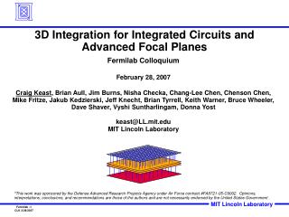
3D Integration for Integrated Circuits and Advanced Focal Planes. Fermilab Colloquium February 28, 2007 Craig Keast , Brian Aull, Jim Burns, Nisha Checka, Chang-Lee Chen, Chenson Chen,

E N D
3D Integration for Integrated Circuits andAdvanced Focal Planes Fermilab Colloquium February 28, 2007 Craig Keast, Brian Aull, Jim Burns, Nisha Checka, Chang-Lee Chen, Chenson Chen, Mike Fritze, Jakub Kedzierski, Jeff Knecht, Brian Tyrrell, Keith Warner, Bruce Wheeler, Dave Shaver, Vyshi Suntharlingam, Donna Yost keast@LL.mit.edu MIT Lincoln Laboratory *This work was sponsored by the Defense Advanced Research Projects Agency under Air Force contract #FA8721-05-C0002. Opinions, interpretations, conclusions, and recommendations are those of the authors and are not necessarily endorsed by the United States Government .
Outline • A brief history of CMOS scaling • Drivers behind “Moore’s Law” and their future outlook • The potential of “Next Generation” technologies beyond silicon CMOS • 3D circuit integration technology and applications • Summary
A Few Metrics • Vacuum tube (early 1900’s) – transistor (1949) – integrated circuit- IC, “chip” (1959) • During the first 10 years of the chip’s development the US government bought the majority of all ICs produced • Today the US Government purchases are a few percent of the market • Today’s microprocessors contain >500 million transistors and occupy ~2-3 cm2 area • Equivalent number of vacuum tubes would cover an area equal to ~250 football fields • First ICs cost ~$120 and contained 10 transistors ($12/transistor), today’s microprocessors cost ~$500 and contain 500,000,000 transistors ($0.000001/transistor) • If this cost scaling was applied to the automobile industry a $100,000 Porsche 911(turbo) would now cost < 1 cent
Single-Crystal Ingot 300 mm Silicon – The Material Enabling the IC(Semiconductor Wafer Preparation) Silicon makes up 25.7% of the earth’s crust Sand Wafer Saw Silicon’s Oxide (SiO2 ) is a KEY attribute of this material’s success
35 Years of CMOS Scalingand Process Improvements IC cross section 10 mm Self-Aligned Gates Self-Aligned Silicides CMP Tungsten Plugs 1 mm Backend Halo Implants Copper Interconnect Low-k Dielectric Strained Silicon 100 nm CMOS Replaces Bipolar For High Performance Computing Technology Node High-k Dielectric??? Frontend CMOS Starts to Replace III-V for Some RF Applications 10 nm Presumed Limit to Scaling Bulk Silicon ???? SOI 1 nm 1970 1980 1990 2000 2010 2020 Year
Drivers Behind Moore’s Law • Smaller feature sizes • Pack more features in given silicon area • Lower cost per function • Smaller transistors are faster • Smaller transistors and wires consume less energy • Bigger chips • More functions on one chip reduces packaging and integration costs, reduces power, improves reliability • Bigger wafer sizes • More chips per wafer; wafer processing cost for bigger wafers rises more slowly than number of transistors/wafer • Manufacturing know-how • Faster machines, higher yields, better tool utilization • More clever device, circuit, and process design • Pack more in a given area, even for a given feature size • “Equivalent scaling”: next generation performance through improved process/materials: SiGe, SOI, strained silicon
Shrinking Feature Size…. Human Hair ~75 m . 0.18 m 180 nm feature . ~40,000 (65-nm node) transistors could fit on cross-section
Current State of the art (>$25 M) 65 nm resolution = 193 nm 0.93 NA (n sin) > 1013 pixels/wafer ~120 300-mm wafers/hour Wafer & mask move 100’s of mm/s during exposure Lithographic Tools ~10’ 4x reduction
Rayleigh criterion for resolution W 30x improvement in resolution over 25 years l from 436 nm to 193 nm sin q from 0.35 to 0.93 k1 from 0.6 to0.35 n from 1 to 1 Now approaching limits l limited by materials and sources sin q < 1 k1 > 0.25 n ??? Optical Lithographic Resolution Slide Courtesy M. Switkes, MIT-LL
Liquid Immersion Interference 27-nm Half Pitch • High-index fluids have been designed and synthesized (n157 = 1.50) • Enable coupling of light from prism to wafer • No need for solid contact – liquid gap of 2 mm is used Immersion fluid Substrate sin q = 0.87 Spacer Prism Si mirror 157 nm light CaF2 Slide Courtesy M. Rothschild, MIT-LL
10 nm 9 nm 9 nm 100 nm 100 nm Optical Lithographyat the Nanometer Level • 9 nm polysilicon gate fabricated • at MITLL 10 nm gold particle attached to Z-DNA antibody. (John Jackson & Inman. Gene [1989] 84, 221-226) 9-nm polysilicon gate on ultra-thin SOI fabricated at MIT-LL using 248-nm PSM optical lithography (2001)
It is likely that we can pattern the smaller feature sizes needed to maintain CMOS scaling…. But will the devices work?
Prognosis For Moore’s Law Benefits • Historically, CMOS scaling has resulted in simultaneous improvements in cost per function, circuit (and system) speed, power consumption, and packing density • Will continued scaling give us the same benefits? Higher Speed? Lower Cost? Lower Power?
Lower CostPrognosis For Moore’s Law Benefits Mask Set Cost • Past • Scaling (s) increases components per unit area as s2 • Wafer size increase gives more chips per wafer • Increasing cost of equipment outweighed by huge increase in number of transistors made per wafer • Future Issues • Skyrocketing equipment costs…Today’s state-of-the-art production facilities cost ~4 billion dollars • NRE (e.g. >$1M mask sets) and productivity issues favor large volume production of “generic” components • Increasing consolidation/pooling of fabrication resources and use of Taiwanese “Super Fabs” TSMC and UMC (China and India next?)
Lower PowerPrognosis For Moore’s Law Benefits • Past • Supply voltage (V) scales as 1/s • Capacitance (C) scales as 1/s • Energy per op scales as CV2 1/ s3 • Voltage scaling from 5V to 1V accounted for 25X reduction in power, just by itself Passive and Active Power vs Gate Length Stove top • Future Issues • Power supply voltage only projected to drop 2X over next 15 years (1.0 to 0.5 V) • Subthreshold device operation? • Scaling energy per op is critical to long endurance battery powered systems and to supercomputers (getting power in and heat out) (~1985) E. J. Nowak, IBM J. Res. & Dev., Vol. 46, No. 2/3, p. 173
Gate Oxide Dielectric* Processor Speed (INTEL)* Gate 4 GHz Channel Research Production Higher SpeedMoore’s Law in Trouble • CPU speed has stalled for the first time in 35 years, with no processor able to break through the “4-Ghz barrier” • Why?...Gate oxide scaling has stopped at Tox~1.2nm in 2003, at the 90-nm technology node (~3-4 monolayers) • Only heroic integration efforts, such as use of strained-Si, have made small dents in the CPU speed barrier • Need a workable High-k gate dielectric in order for performance scaling to continue *D. A. Muller, Nature Materials V 4, pg. 645 (2005)
Future High PerformanceDevice “frontend” Possibilities • Continue with Si CMOS. Some possible alternative silicon futures are: • CPU speed could be maxed out – future improvements will come from reduced cost and higher density and integration “multi-core” chips • High-k could save the day – if not tomorrow, maybe in 10 years • A perfect high-k gate dielectric will enable CPU speeds to increase until the next tunneling limit (source-to-drain) at the 10nm-node • Changes in device architecture could take the pressure off the gate oxide, and CPU speed will continue to advance at a slower rate • FDSOI and FinFET lets Tsi scale instead of Tox No high-k With high-k Intel - components research (IEDM2003)
Future Possibilities (Cont’d) • A future with transistors, but without silicon: • Germanium-based devices • Improved mobility, at the expense of many other semiconductor properties • Carbon-based devices. Several flavors: • Carbon nanotubes: Have better device properties than Si, but are very difficult to integrate (thus far) • Graphite devices: Difficult to turn off • Molecular devices: Have not been demonstrated to work better than Si
Future Possibilities (Cont’d) • A future without transistors: • Josephson-junction-based logic • Demonstrated and works, but at 4K • Real speed and power advantages unclear • Quantum Computation • Can’t execute traditional code, even theoretically • But can solve Schrödinger's equation blazingly fast, and factor very large numbers • Cross Point Arrays – nanowire, molecular • Too simple for general purpose logic, if complexity is increased to meet logic constraints the result is a transistor • MEMS, protein, spin logic – too early to evaluate
Estimated Performance Potential Technology Roadmap Silicon devices Research Required Alternate Si Structures FDSOI FinFET Perfect high-k Germanium devices Carbon-nanotube devices Graphite devices Molecular devices Spintronics – no evaluation possible, insufficient experimental data Possible global directions for high performance logic technology in the next 20 years considered in this study, and graphical summary of their evaluations when possible
S VDS = -0.1,-0.2,-0.3 V L ~ 50 nm 100 nm SWNT -6 10 (A) D S L~30 nm VDS=-0.3 V DS -8 -I 10 -1 0 V (V) G Future Technology Highlights:Carbon Nanotubes (CNTs) 1 nm (Drawing and AFM from CEA website) • Example of experimental CNT device from Stanford • Features: metal gate, high-k dielectric, metal source/drain • High performance: 10x Si device of same geometry • Putting tubes were they are needed is a problem REF: A. Javey, et al. Nano Lett, 2004.
Future Technology HighlightsThin Graphite - Graphene REF: K.S Novoselov et al., Science, V. 306, 22 October 2004, p. 666 • Graphite has high mobility of >10,000 cm2/Vs (~15x Si) • Graphite is a semi-metal (semiconductor with band-gap of 0eV) • Difficult to turn off, a fundamental challenge • Proven planar techniques could be used in fabrication • Planar geometry of devices eliminates majority of integration difficulties of carbon nanotubes • MIT-LL has begun to explore this material system • Leveraging layer transfer, materials, and microelectronic fabrication expertise at the Laboratory Few monolayer graphite device SEM and electrical characteristics at T=70K
The Integrated Circuit Interconnect “backend” Challenge Relative Wiring Delay vs Feature Size* Typical Process Cross-Section* Cu Metal Low-k Dielectric Global Interconnect (up to 5) Intermediate Interconnect (up to 8) Local Interconnect Active Device *From 2005 International Technology Roadmap for Semiconductors (ITRS)
2D Very Long Wires 3D Shorter Wires Wire Length Distribution in 90 nm Node IBM Microprocessor* • >50% of active power (switching) dissipation is in microprocessor interconnects • >90% of interconnect power is consumed by only 10% of the wires *After K. Guarini IBM Semiconductor Research and Development Center
300 From 2003 ITRS Roadmap 700 MHz 250 1.25 GHz 200 2.1 GHz Process Technology (nm) 150 6 GHz 10 GHz 100 13.5 GHz 50 (20 mm x 20 mm Die) 0 1995 2000 2005 2010 2015 Year Range of Wire in One Clock Cycle* • 3D Integration increases accessible active devices *After S. Amarasinghe, MIT Laboratory for Computer Science and Artificial Intelligence
Motivation for 3-D Circuit Technology Reduced Interconnect Delay High Bandwidth m-Processors Exploiting Different Process Technologies Advanced Focal Planes Mixed Material System Integration
Pad-Level “3D Integration”Die Stacking Stacked-Die Wire Bonding Stacked Chip-Scale Packages 1 mm ChipPAC, Inc. Tessera, Inc. In Production!
Tier-1 10 mm 3D-Vias Tier-3 3D-Vias Tier-2 Tier-1 10 mm 10 mm Tier-2 Photo Courtesy of RTI Approaches to High-Density 3D Integration(Photos Shown to Scale) Two-layer stack with insulated vias through thinned bulk Si Bump Bond used to flip-chip interconnect two circuit layers Three-layer circuit using MIT-LL’s SOI-based vias
SOI Cross-Section Bonding Layer Buried Oxide Handle Silicon Oxide ~6 mm ~675 mm Advantages of Silicon-on-Insulator (SOI) for 3-D Circuit Integration • The electrically active portion of an integrated circuit wafer is < 1% of the total wafer thickness • Buried oxide layer in SOI provides ideal etch stop for wafer thinning operation prior to 3D integration • Full oxide isolation between transistors allows direct 3D via formation without the added complexity of a via isolation layer • SOI’s enhanced low-power operation (compared to bulk CMOS) reduces circuit stack heat load
3-D Circuit Integration Flow-1 • Fabricate circuits on SOI wafers • SOI wafers greatly simplify 3D integration • 3-D circuits of two or more active silicon layers can be assembled Buried Oxide Wafer-1 can be either Bulk or SOI Handle Silicon Wafer-1 Buried Oxide Wafer-2 Handle Silicon Buried Oxide Wafer-3 Handle Silicon
Wafer-2 Handle Silicon Buried Oxide Wafer bond Wafer-1 3-D Circuit Integration Flow-2 • Invert, align, and bond Wafer-2 to Wafer-1 • Remove handle silicon from Wafer-2, etch 3D vias, deposit and CMP damascene tungsten interconnect metal “Back Metal(s)” IC2 Tier-2 Concentric 3D Via Tier-1 Wafer-1 Handle Silicon
IC3 IC3 Tier-3 Tier-3 IC2 IC2 Tier-2 Tier-2 Tier-1 Tier-1 Wafer-1 Wafer-1 Handle Silicon Handle Silicon 3-D Circuit Integration Flow-3 • Invert, align, and bond Wafer-3 to Wafer-2/1-assembly, remove Wafer-3 handle wafer, form 3D vias • Etch Bond Pads IEEE Trans. on Electron Devices, Vol. 53, No. 10, October 2006
T(oC) 500 200 350 350 300 300 250 250 150 150 450 450 400 400 10000 Surface Energy (mJ/m2) 1000 1 hr. 1 hr. o 275 275oC, 10 hr C, 10 h 10 hr. 10 hr. Ea=0.14eV E =0.14eV a 100 1.2 1.2 1.4 1.4 1.6 1.6 1.8 1.8 2.0 2.0 2.2 2.2 2.4 2.4 1000/T (oK-1) 3D-Specific Enabling Technologies Low temperature oxide-bond process Bond Interface Precision wafer-wafer alignment High-density 3D-Via
4 x 4 Tiled Array (mock-up) 4-Side-Abuttable Mosaic Focal Planes • Tier-1: 100% fill-factor silicon photodetector layer • Tier-2: CMOS address and readout layer 1024 x 1024 Image Imager Cross-Section (8 mm Pixel Pitch) Image acquired at 10 frames/sec (Background Subtracted, Pixel Yield > 99.9%,3.8M transistors) Presented at 2005 ISSCC
Completed Pixel Cross-Sectional SEM 3D Via Tier-3: 1.5V SOI CMOS Layer Transistors 3D Via Tier-2: 3.5V SOI CMOS Layer 10 mm Tier-1: 30V Back Illuminated APD Layer 10 mm 3D-Integrated, 3-Tier Avalanche Photodiode Focal Plane • VISA laser radar focal plane based on single-photon-sensitive Geiger-mode avalanche photodiodes • 64 x 64 format • 50-mm pixel size To-Scale Pixel Layout of Completed 3-tier Laser Radar Focal Plane Tier-3 High-Speed Counter Tier-2 APD Drive/Sense Circuitry Tier-1 Avalanche Photodiode (APD) ~250 transistors/pixel (50 mm x 50 mm) Presented at 2006 ISSCC
First 3-D IC Multiproject Run (Three 180-nm, 1.5 volt FDSOI CMOS Tiers) 22 mm Completed 3DL1 Die Photo • Leverages MIT-LL’s established 3D circuit integration technology • Low temperature oxide bonding, precision wafer-to-wafer overlay, high-density 3D interconnect • Preliminary 3D design kits developed • Mentor Graphics – MIT-LL, Cadence – NCSU, Thermal Models – CFRDC • Design guide release 11/04, fab start 6/05, 3D-integration complete 3/06 Concepts being explored in run: 3DL1 Participants (Industry, Universities, Laboratories) 33 Designs
Back Metal Tier-3: Transistor Layer Tier-3: 180-nm, 1.5V FDSOI CMOS 3D-Via Stacked Vias Metal Fill Tier-2: Transistor Layer Oxide Bond Interface 3D-Via Tier-2: 180-nm 1.5V FDSOI CMOS 3D-Via 3-Level Metal Oxide Bond Interface 10 mm Tier-1: Transistor Layer Tier-1: 180-nm, 1.5V FDSOI CMOS Cross-Section of 3-Tier 3D-integrated Circuit (DARPA 3DL1 Multiproject Run) 3 FDSOI CMOS Transistor Layers, 10-levels of Metal
5 mm 5 mm 5 mm 3D Technology Improvements(DARPA 3DL1 Multiproject Run) High-Yield on >5000-link Scaled 3D-via Chains • 3D technology enhancements successfully demonstrated in 3DL1 Run • Stacked 3D-vias for electrical and thermal interconnect • 2X reduction in 3D-via size • Improved tier-to-tier overlay Conventional Scaled Stack 3D-vias demonstrated >95% yield on 4800 link chains Stacked 3D-via resistance ~1W Can be used as thermal vias ~0.5 mm 3s Tier-to-Tier Registration 99-Stage Ring Oscillator @1.5V
3D Ring Oscillator Cross-Sectional SEM Tier-3: FDSOI CMOS Layer 3D Via Stacked 3D Via 3D Via Tier-2: FDSOI CMOS Layer Transistors 5 mm Tier-1: FDSOI CMOS Layer Stage Delay (ps) 99-Stage Ring Oscillator @1.5V Power Supply (V) 3-Tier, 3D-Integrated Ring Oscillator (DARPA 3DL1 Multiproject Run) • Functional 3-tier, 3D-integrated ring oscillator • Uses all three active transistor layers, 10 levels of metal and experimental stacked 3D-vias • Demonstrates viability of 3D integration process
3D IC Multiproject Run Highlights (a) • RPI, Jack McDonald (PI) • Designed high-bandwidth 3D SRAM for high-performance computing applications • Demonstrated first functional 3D-integrated, 3-tier memory • Stanford Univ.,Sang-Min Lee, Bruce Wooley (PI) • Designed and demonstrated high dynamic range (18-19 bit) high frame rate (3000 fps) 3D ADC for LWIR focal plane array readouts • Reduced pixel size for complex readout to 50 mm x 50 mm
Output Eye diagram Input vs Output 3D IC Multiproject Run Highlights (b) • UCLA, Frank Chang (PI) • Designed low power, low BER 10Gbps capacitor-coupled vertical Interconnects for 3D-IC • Demonstrated Baseband Impulse Shaping Interconnect (BISI) and self-synchronized RF Interconnect (RFI) at >11 GHz with BER < 1x10-14 • >10x lower energy/bit and >3x faster than previously reported 180-nm 2D communication circuits • NRL-Cornell-BAE,Maxim Zalalutdinov (PI) • Designed 3D CMOS-integrated high frequency, high quality factor micromechanical resonators • Demonstrated tuning fork and slot resonators at 34MHz with Q = 4700 RFI Test @ 12.5 GHz data rate Post Process Released Resonator
3D IC Multiproject Run Highlights (c) • Cornell Univ., Sandip Tiwari (PI) • Designed full range of 3D test structures and circuits • Characterized 3D heat dissipation • Demonstrated functional asynchronous 3D FPGA • Demonstrated low voltage adaptive analog circuits with backgating • Demonstrated RF cross-talk reduction through 3D-integrated ground planes • Yale Univ., Eugenio Culurciello (PI) • Designed 3D integrated detector sensitive to intensity, contours, and motion • Demonstrated functionality of single and multiple tier photo detectors Asynchronous 3D FPGA 3D pixel view three 3D vias per pixel
Thermal characterization structures included in 3DL1 Multiproject Run Measure temperatures in stack Explore thermal sink paths through buried oxide (BOX) vias and “Back-metal” hear sinks Calibrate thermal modeling tools Temperature Measurement Results from 3DL1 Multiproject Run 3D Temperature Characterization Structure
3DM2 Multiproject Run(3 Active Tiers, 11 levels of Metal) • 3DM2 includes 2 “digital” 180-nm FDSOI CMOS tiers and 1 RF 180-nm FDSOI CMOS tier • 11 metal layers including: • 2-mm-thick RF Backmetal • Tier-2 Backmetal • Second 3D Multiproject Design Schedule (3DM2) • 3DM2 announcement (Mar 06) • Contributor selection (Apr 06) • Design guide release (Apr 06) • Submission deadline (November 06)
150-mm-diameter InP wafer with oxide-bonded circuit layer transferred from silicon wafer 3D-Integration with III-V Detectors • Enables extension of 3D-integration technology to higher density, longer wavelength focal plane detectors • Tight pixel-pitch IR focal planes and APD arrays • InGaAsP (1.06-mm), InGaAs (1.55-mm) • High-yield, 3.4 mm pitch 3D-via chains demonstrated Presented at 2006 IPRM
SummaryA Few Closing Remarks… • Transistor feasibility has been demonstrated to below ~10 nm gate lengths • “Conventional” CMOS (Bulk, SiO2 gate oxide, poly gates) faces significant challenges to scale below 45nm-node • Ultra-thin-body SOI, FinFET, Dual-Gate, Metal Gate, High-k • No new device technology has yet emerged that is expected to dethrone silicon CMOS • Moore’s Law scaling is showing its age and could run into serious speedbumps in the next few years (including economics), but the 2020 roadmap is theoretically feasible • Process technology improvements are no longer the performance drivers • Future performance improvements will most likely come through circuit, system architecture, and software advancements • Initial 3D technology demonstrations (at MIT-LL) are centered around advanced focal plane architectures • This is the “low hanging fruit” • Full impact of 3D integration is far from being realized, but has the potential of revolutionizing the design architecture of future circuits and systems • Potential application areas include: High-end focal planes, FPGAs, Dense memory, memory on processor, mixed signal systems, mixed material systems