Download
1 / 85
870 likes | 1.09k Vues
16 Tap FIR Filter. Omar F. Mousa/Chintan Daisa Professor: Scott Wakefield. Design Objectives. To have a register based storage of 16 latest input values and the 16 impulse response coefficients on-chip. To utilize a clocked architecture to synchronize input and output values.

E N D
16 Tap FIR Filter Omar F. Mousa/Chintan Daisa Professor: Scott Wakefield
Design Objectives • To have a register based storage of 16 latest input values and the 16 impulse response coefficients on-chip. • To utilize a clocked architecture to synchronize input and output values. • Reduce the Number of Multiplier and Adder needed that is Optimize area and Power and cost. • By Achieving the above the speed will not be compromised
Design Objectives • Future scalability for input data as well as coefficient bits. • Signed or unsigned input data as well as coefficients. • Fast MAC operation on signed or unsigned data with future scalability. • Synchronization of Input/Output data • Configurable Output Precision
Design Objectives • 16 taps of delay line. • 8 bits of Input/Output bit resolution • Burst mode of data transfer at Input supporting 32 elements of the desired resolution in one burst Main Issue of concern when designing FIR Filter • Sharp Response • Number of Taps • Numerical Precision • Fully Parallel
Advantages and Disadvantages • Advantages: • Always stable (assume non-recursive implementation). • Quantization noise is not much of a problem. • Transients have a finite duration. • Disadvantages: • A high-order filter is generally needed to satisfy the stated specification – so more coefficients are needed with more storage and computation.
Review of discrete-time systems x[k] y[k] Linear time-invariant (LTI) systems • Causal systems: for all input x[k]=0, k<0 -> output y[k]=0, k<0 • Impulse response : input 1,0,0,0,... -> output h[0],h[1],h[2],h[3],... input x[0],x[1],x[2],x[3] -> output y[0],y[1],y[2],y[3],...
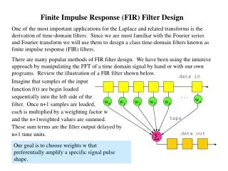
Overview FIR filter equation y[n] = x[n] * h [n] where n is the number of “taps” or coefficients in the FIR filter. For a 16-tap FIR filter y[n] = a0x[n] + a1x[n-1] + a2x[n-2] + a3x[n-3]+…+ a15x[n-15]
Different Filter Representations Difference equation Recursive computation needs y[-1] and y[-2] For the filter to be LTI, y[-1] = 0 and y[-2] = 0 Transfer function Assumes LTI system Block Diagram Representation x[k] y[k] UnitDelay 1/2 y[k-1] UnitDelay 1/8 y[k-2]
Discrete-Time Systems • Z-Transform:
Discrete-Time Systems `Popular’ frequency responses for filter design : low-pass (LP) high-pass (HP) band-pass (BP) band-stop multi-band …
Digital Filter Specifications • For example the magnitude response of a digital lowpass filter may be given as indicated below
Structured Streams • Hierarchical Structures: • Pipeline • SplitJoin • Feedback Loop
Different Strategies • Map filter per tile and run forever • Pros: • No filter swapping overhead • Reduced memory traffic • Localized communication • Tighter latencies • Smaller live data set • Cons: • Load balancing is critical • Not good for dynamic behavior • Requires # filters ≤ # processing elements
Discrete-Time Systems `FIR filters’ (finite impulse response): • Moving average filters (MA) • N poles at the origin z=0 (hence guaranteed stability) • N zeros (zeros of B(z)), `all zero’ filters • corresponds to difference equation • Impulse response
Speeding Up FIR Filter • FIR speed-up • y(0) = c(0)x(0) + c(1)x(-1) + c(2)x(-2) + . . . + c(N-1)x(1-N); • y(1) = c(0)x(1) + c(1)x(0) + c(2)x(-1) + . . . + c(N-1)x(2-N); • y(2) = c(0)x(2) + c(1)x(1) + c(2)x(0) + . . . + c(N-1)x(3-N); • . . . • y(n) = c(0)x(n) + c(1)x(n-1) + c(2)x(n-2)+ . . + c(N-1)x(n-(N-1)); • Run MAC at double frequency, read two 32-bit numbers • FIR filtering: two outputs in parallel • Two outputs = 4N reads, 2N MAC’s, 2 writes
Direct Form Realization u[k] u[k-1] u[k-2] u[k-3] u[k-4] bo b1 b2 b3 b4 x x x x x y[k] + + + +
Retiming FIR Filter Realizations u[k] u[k-1] u[k-2] u[k-3] u[k-4] bo b1 b2 b3 b4 x x x x x y[k] + + + + • Select subgraph (shaded) • Remove delay element on all inbound arrows • Add delay element on all outbound arrows
Retiming u[k] u[k-1] u[k-2] u[k-3] bo b1 b2 b3 b4 x x x x x y[k] + + + +
Four Tap Direct Form Realization u[k] u[k-1] u[k-3] u[k-2] bo b1 b2 b3 x x x x + + + y[k]
Transposed Direct-Form Realization u[k] b1 b2 b3 b4 x x x x bo x y[k] + + + +
Lattice Form Realizations u[k] u[k-1] u[k-2] u[k-3] u[k-4] bo b1 b2 b3 b4 x x x x x b4 b3 b2 b1 bo x x x x x y[k] + + + + ~ y[k] + + + +
FIR Filter Realizations x x x x x x x x x + + + + + + + + ~ y[k] Lattice Form u[k] bo y[k] ko k1 k2 k3 i.e. different software/hardware, same i/o-behavior
Efficient Direct Form Realization u[k] + + + + + Efficient Direct-Form realization. bo b1 b2 b3 b4 x x x x x y[k] + + + +
Pin Diagram Vdd Gnd x[0] Drive x[1] y[0] ….. y[1] x[15] 16-bit 16-tap FIR Filter y[2] a[0] y[3] a[1] y[4] ….. y[5] a[15] y[6] Reset …. y[31] Coeffin Din Clk • Synthesis using Synopsys Design Compiler • Initial Target Frequency: 100 MHz (typical)
Specifications Input Specifications • 16-bit unsigned integers for data inputs. • 16-bit unsigned integers for coefficients. Output Specifications • 32-bit unsigned integer output.
System Components • Memory - Input and Coefficient • Control - Mod-4 and Mod-8 counters - 3-8 Decoder - Combinational logic • Multiplier - Radius-8 Booth multiplier - Multiplier register • Adder - 9-bit Carry Save adder - Adder register • Output Register
Specifications Drive Signal(Output Signal) • A new output is available. • Inputs or coefficients to be applied only when Drive is asserted. • Coefficients • Any coefficient changed implies a new filter definition. • Input Memory cleared – new data to be entered.
Specifications System Clock • One clock-cycle for the filter = 32 input clock pulses. • One Tap-cycle = 8 input clock pulses described as 8 phases. • 4 such Taps for each output. System Reset • Active High
System Timing • mod8 counter states F0 F1 Input or Coefficient memory enable F2 Multiplier propagation delay F3 Multiplier propagation delay F4 Multiplier Register enable F5 Add Register Enable F6 Output Register Enable F7
System Timing Strategy • Two phase clocking • Generation of internal lower frequency clocks using mod-4 and mod-8 counters • Each state of mod-4 counter used for computation of one filter tap • Output available at the end of one cycle of mod-4 counter
2-Parallel FIR Filtering Structure x(2k) y(2k) H0 + H1 x(2k+1) y(2k+1) H0 + H1 D z-2
Hardware-Efficient 2-Parallel FIR Filter x(2k) y(2k) H0 + y(2k+1) H0+H1 + + + x(2k+1) H1 D z-2 • Y0 = X0 H0 + z-2X1H1 • Y1 = X0 H1 + X1 H0 = (H0 + H1) (X0 + X1) – H0X0 – H1X1
Savings in the New Structure • Originally, • 2N multiplications + 2(N-1) additions for two inputs • In the new structure • 3*(N/2) = 1.5N multiplication • 3(N/2 –1) + 4 = 1.5N + 1 additions
Design Flow FIR 16 Tap Delay VHDL Deign Entry Functional Verification Synthesis EDIF Timing Verification Floor planning SDF PDEF Parasitic PDEF Physical Verification Place & Route
The FIR Filter • Implementation of 16 Tap FIR Filter, the coefficients are represented as fixed point 16-bits 2’s complement numbers. It is assumed that either or both of the coefficients and data are fractional numbers.
FIR Filter(Critical Path) • In order to save area and improve the critical path performance, we decided to add the 12-bit sum and carry results of the multiplier during the accumulation operation. Therefore, the adder has to add three 12-bit numbers. To do that, the first stage of the adder is a 3-to-2 combiner, which is just a CSA. The next stage is a CPA (Carry Propagate Adder) arranged in a static Manchester carry chain form. The chain is divided into four sections, each one has three carry stages. Buffers are used between sections to reduce the overall delay.
Survey of Multiplier • Combinational Multiplier: uses n adders, eliminates registers:
Multiplier Design 44 multiplication X3 X2 X1 X0 multiplicand Y3 Y2 Y1 Y0 multiplier X3Y0 X2Y0 X1Y0 X0Y0 X3Y1 X2Y1 X1Y1 X0Y1 X3Y2 X2Y2 X1Y2 X0Y2 X3Y3 X2Y3 X1Y3 X0Y3 Z7 Z6 Z5 Z4 Z3 Z2 Z1 Z0 Result P.P.
Radix-2 Unsigned Multiplication Use a single n-bit adder, three registers (P, A, B), and a testing circuit for A0 Initialization: Place the unsigned numbers in registers A and B. Set P to zero. 1: If A0 is 1, then register B, containing bn-1bn-2...b0 is added to P; otherwise 00...00 (nothing) is added to P. The sum is placed back into P. 2. Shift register pair (P, A) one bit right. The last bit of A is shifted out (not used).
Array Multiplier • Array multiplier is an efficient layout of a combinational multiplier. • Array multipliers may be pipelined to decrease clock period at the expense of latency.
Array Multiplier Organization 0 1 1 0 x 1 0 0 1 0 1 1 0 + 0 0 0 0 0 0 1 1 0 + 0 0 0 0 0 0 0 1 1 0 + 0 1 1 0 0 1 1 0 1 1 0 Multiplicand Multiplier skew array for rectangular layout Product
Unsigned Array Multiplier x2y0 x1y0 x0y0 0 0 x1y1 x0y1 + + x1y2 x0y2 + + xny0 0 + + P(2n-1) P0 P(2n-2)
Array Multiplier Organization Array Multiplier cell Pin Xi Yi Xi Yi Pin Cout FA Cin Cin Cout Pout Pout M-1 Critical Path N-1 P.P tmult(M-1) tcarry +(N-1) tsum + tand For small tmult, tcarry tsum Beneficial to make tcarry = tsum Differential Logic (DCVS)
Architecture of Array Multiplier X3 X2 X1 X0 Y0 Y1 Y2 Y3 Z0 Z1 Z2 × HA × HA × HA × HA Z7 Z6 Z5 Z4 Z3
Advantages of Array Multiplier p9 a4x4 p8 a4x3 a3x4 p7 a4x2 a3x3 a2x4 p6 a4x1 a3x2 a2x3 a1x4 p5 a4 x4 a4x0 a3x1 a2x2 a1x3 a0x4 p4 a3 x3 a3x0 a2x1 a1x2 a0x3 p3 a2 x2 a2x0 a1x1 a0x2 p2 a1 x1 a1x0 a0x1 p1 a0 x0 a0x0 p0 • Array multipliers • Partial product generation and accumulation are merged • Identical cells • High-rate pipelining
Array Multiplier • Array multiplier for Unsigned numbers a4x0 a3x0 a2x0 a1x0 a0x0 0 0 0 0 a4x1 a3x1 a2x1 a1x1 a0x1 a4x2 a3x2 a2x2 a1x2 a0x2 a4x3 a3x3 a2x3 a1x3 a0x3 a4x4 a3x4 a2x4 a1x4 a0x4 0 p9 p8 p7 p6 p5 p4 p3 p2 p1 p0
Array Multiplier for Two’s Complement z y II x s c x + y - z 2c - s 0 0 0 0 0 0 0 1 0 1 0 1 0 1 1 0 1 1 0 0 1 0 0 1 1 1 0 1 0 0 1 1 0 1 0 1 1 1 1 1 • type I cell • ordinary full adder • type II cell • x + y - z = 2c - s s = (x + y - z) mod 2 c = [(x + y - z) + s] / 2 • type I cell with inverted z and s z=1-z’, s=1-s’ weight = -1
Array Multiplier for Two’s Complement z y weight = -1 II’ x s c weight = -2 • type II’ cell : • - x - y + z = - 2c + s Þ x + y - z = 2c - s Þ identical to the type II cell
Architecture of Carry-Save Multiplier Carry-Save Multiplier carry propagation : diagonally downwards instead of to left Requires additional adder (vector-merging adder) You can make this final adder very fast using CLA or CSA scheme 44 multiplier ripple-carry based multiplier
Architecture of Carry-Save Multiplier Critical path Vector-merging adder carry-save multiplier tmult=(N-1) tcarry + tand + tvma Carry-Save Multiplier (44)