ROMs and Latches: Memory Implementations and Logic Circuits
230 likes | 263 Vues
Understand ROM implementation technology, memory storage devices, and latch-based sequential circuits. Learn optimization techniques, speed-up methods for ROMs, and dynamic disciplines for latch functionality.

ROMs and Latches: Memory Implementations and Logic Circuits
E N D
Presentation Transcript
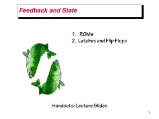
Feedback and State • ROMs • 2. Latches and Flip-Flops Handouts: Lecture Slides
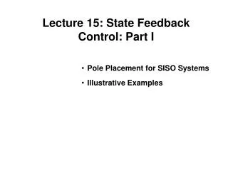
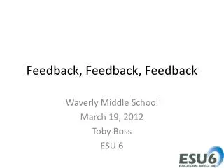
This ROM stores 16 bitsin 8 words of 2 bits. General Purpose “Table-Lookup” Devicea.k.a Read-Only Memory (ROM) Decoder A B Cin Fixed “AND plane” 0 1 2 3 7 4 5 6 S Configurable “OR plane” Cout Configurable Selector Made from PREWIRED connections , and CONFIGURABLEconnections that can be either connected or not connected
ROM Implementation Technology PFET with gate tied to ground = resistor pullup that makes wire “1” unless one of the NFET pulldowns is on. A Hardwired AND logicProgrammable OR logic Advantages: - Very regular design Problems: - Active Pull-ups (Static Power) - Long metal wires, large capacitance - Slow B Cin S Cout
000 001 The best way to accomplish this is to build square arrays: 010 011 100 00 101 01 110 10 A 111 B 11 CIN A 0 1 S COUT B 0 1 CIN 2D Addressing: Standard for ROMs, RAMs, … S COUT Speeding up ROMs Minimize the capacitances of those long wires running through the array.
T U V W X Y Z Example: 7-sided Die We want to construct a readout displaying the following symbols: An array of LEDs, labeled as follows, can be used to display the outcome of the die:
T U V W X Y Z ROM-Based Design • Once we’ve written out the truth table we’ve basically finished the design • Possible optimizations: • - Eliminate redundant outputs • - Addressing tricks Truth Table for a 7-sided Die
No output depends onthis product term T U V W X Y Z A Simple ROM implementation A B C That was easy but there is clearly some waste. - unused products - over-specified terms T/Z U/Y V/X W
Combinational Logic Digital StateOne model of what we’d like to build Next State Memory Device Current State LOAD Input Output • Plan: Build a Sequential Circuit with stored digital STATE – • Memory stores CURRENT state, produced at device output • Combinational Logic computes • Next state (from input, current state) • Output bit (from input, current state) • State changes on LOAD control input
VOUT VIN Not affected by noise Feedback constraint: VIN = VOUT VTC for inverter pair VOUT Three solutions: w two end-points are stable w middle point is unstable VIN We’ll get back to this! Memory/Storage Device Using Feedback IDEA: use positive feedback to maintain storage indefinitely. Result: a bistable storage element
“state” signal appears as both input and output G 0 0 1 1 D -- -- 0 1 QIN 0 1 -- -- QOUT 0 1 0 1 Q Q stable D Q follows D G Settable Storage Element It’s easy to build a settable storage element (called a latch) using a MUX: A 0 Y B 1 S
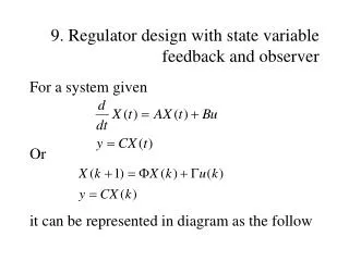
D G V1 V2 V2 V1 Q D Q G tpd tpd New Device: D Latch G=1: Q follows D G=0: Q holds Q’ 0 Q D 1 G G=1:Q Follows D, independently of Q’ G=0:Q Holds stable Q’, independently of D
“glitch” or “hazard” Glitch at Q can cause Y to fall and change state Want Q to stay at 1 Hazardous D-Latch Qold = 1 initially Y Q G D = 1 Z Only one input G changes to latch
1 What if D and G change 1 0 at the same time? Lenient D-latch D DG Q G GQ DQ GQ 00 01 11 10 D No problem for all single input transitions 0 1 0 0 0 1 1 1 0 1
Setup time = ts ts D Q Hold time = th th G D must not change in this region to ensure single input change to latch Timing Specifications for D-Latch tpd G Q Flow through tcd G Q G D old Q Q
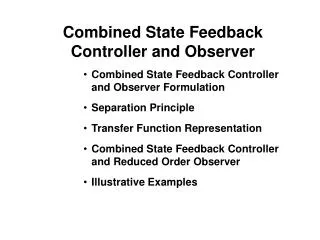
V2 V2 0 A Q Y D 1 G tsetup thold D G Q tpd tpd tpd Dynamic Discipline for Latch D Stable tpd Q’ To reliably latch V2: • Apply V2 to D, holding G=1 • After tpd,V2 appears at Q=Q’ Dynamic Discipline for Latch • After another tpd, Q’ & D both valid for tpd; will hold Q=V2 independently of G tsetup = 2 tpd: interval prior to G transition for which D must be stable & valid • Set G=0, while Q’ & D hold D=Q thold = tpd: interval following G transition for which D must be stable & valid • After another tpd,G=0 and Q’ are sufficient to hold Q=V2 independently of D
Next State D Q G Current State Input Output Combinational Logic Latch-Based Sequential Circuit • Plan: Build a Sequential Circuit with one bit of STATE – • Single latch holds CURRENT state • Combinational Logic computes • Next state (from input, current state) • Output bit (from input, current state) • State Q changes when G = 1
New State D Q G Current State Input Output Combinational Logic Combinational Cycles 1 • When G=1, latch is Transparent… • … provides a combinational path from D to Q. • Need a G=1 PULSE for this to work! Pulse too wide combinational cyclePulse too narrow not enough time for D to change Q Two-sided time bounds make this virtually unimplementable
Flaky Control Systems Here’s a strategy for saving a few bucks on the Pike
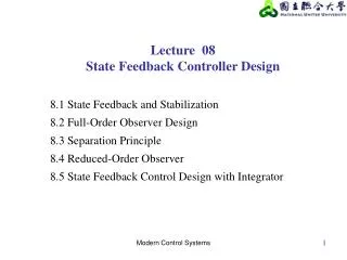
The gate of this latch is open when the clock is low The gate of this latch is open when the clock is high • Observations: • only one latch “transparent” at any time: • master closed when slave is open • slave closed when master is open • no combinational path through flip flop • w Q only changes shortly after 0 1 • transition of CLK, so flip flop appears • to be “triggered” by rising edge of CLK D Q D Q G Edge-triggered Flip Flop D D Q Q D Q master slave G CLK CLK
Latches and Flip-Flops Q D is like a toll-gate G Q D is like an air-lock
New State Flip- Flop Current State Clock Input Output Combinational Logic Discrete-Time Sequential Circuit No combinational cycle! • Active Clock Edges punctuate time --- • Discrete Clock periods, state variables, specifications • Dynamic discipline for flip-flop corresponds to various timing constraints
Next Time: Clocking Dilbert : S. Adams