Download
1 / 20
210 likes | 373 Vues
Design and Implementation of a WiMAX Baseband Processor. Student: 莊宜豐. Outline. Introduction WiMAX FPGA Architecture Design Transmitter Architecture Receiver Architecture Conclusions. Introduction.

E N D
Design and Implementation of a WiMAX BasebandProcessor Student:莊宜豐
Outline • Introduction • WiMAX • FPGA • Architecture Design • Transmitter Architecture • Receiver Architecture • Conclusions
Introduction • It provides one baseband processor. First, building the models of the transmitter, the wireless channel. • Using VHDL language to design and implement the circuit. Finally, verifying the circuit on FPGA.
FPGA(Field Programmable Gate Array ) • Performance • Design Time • Design Cost • Manufacturing Cost • Short Design Time
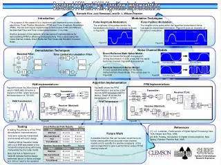
Frame Detection • Frame Synchronization of the (Long/Short) Preamble • (Fine/Coarse) Frequency Synchronization • Fast Fourier Transform (FFT) • Channel Estimation • Equalizer • Channel Tracking • Timing Synchronization
Five steps for deriving correct the signals. The flow diagram of the receiver. (Step 1)
Summary: • For step 1, this step would save a lots power consumptions. • For step 5, the proposed receiver turn four blocks off until next subframe arriving so that it also saves a lots power consumptions. • Therefore, it is more suitable for the mobile communication system.
Conclusions • In this thesis, a baseband processor conforming to IEEE 802.16-2004 OFDM specifications are proposed. There are two main components in the inner receiver. • In the software simulation and prototyping measurement, all results are functionally correct and provide satisfactory performance.
Circuit Design Channel Estimator