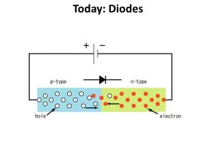
Diodes
Diodes. Transistor Types?. MOSFET Circuit Symbols. (g) and (i) are the most commonly used symbols in VLSI logic design. MOS devices are symmetric. In NMOS, n + region at higher voltage is the drain. In PMOS p + region at lower voltage is the drain. NMOS Transistor.

Diodes
E N D
Presentation Transcript
MOSFET Circuit Symbols • (g) and (i) are the most commonly used symbols in VLSI logic design. • MOS devices are symmetric. • In NMOS, n+ region at higher voltage is the drain. • In PMOS p+ region at lower voltage is the drain.
MOSFET Bias Analysis Example Since VGS < VTNfor VGS = -2.71 V and MOSFET will be cut-off, Problem: Find Q-pt (ID, VDS) Approach: Assume operating region, find Q-point, check to see if result is consistent with operation region VDS > VGS -VTN . Hence saturation region assumption is correct. Q-pt: (34.4 mA, 6.08 V) with VGS = 2.66 V
Bias Analysis Example 2 (Two-Resistor biasing for PMOS Transistor) Also Since VGS = -0.369 V is less than VTP = -2V, VGS = -3.45 V ID = 52.5mA and VGS = -3.45 V Assumption:IG = IB = 0, transistor is saturated (since VDS =VGS) Analysis: Hence saturation assumption is correct. Q-pt: (52.5 mA, -3.45 V)
MOSFET as a Current Source • Ideal current source gives fixed output current regardless of voltage across it. • MOSFET behaves as as an ideal current source if biased in the pinch-off region (output current depends on gate-source terminal voltage).
NMOS Current Mirror Assumption:M1 and M2 have identical VTN, Kn’, l and W/L and are in saturation. Thus, the output current precisely mirrors the reference current if VDS1 = VDS2.
MOS Current Mirror Ratio Thus, the ratio between IO and IREF can be modified by changing the W/L ratios of the current mirror transistors (ignoring differences due to VDSmismatch)
N-Channel JFET i-v Characteristics Output Characteristics Transfer Characteristics
npn Bipolar Transistor: Forward Characteristics Base current is given by is forward common-emitter current gain Emitter current is given by is forward common- base current gain Forward transport current is IS is saturation current In this forward active operation region, VT = kT/q =0.025 V at room temperature
i-v Characteristics of Bipolar Transistor: Common-Emitter Output Characteristics For iB = 0, transistor is cutoff. If iB > 0, iC also increases. For vCE > vBE, npn transistor is in forward-active region, iC = bFiB is independent of vCE. For vCE < vBE, transistor is in saturation. For vCE < 0, roles of collector and emitter reverse. Chap 5 - 12
Operation Regions of Bipolar Transistors Binary Logic States Chap 5 - 13
i-v Characteristics of Bipolar Transistor: Common-Emitter Transfer Characteristic Defines relation between collector current and base-emitter voltage of transistor. Almost identical to transfer characteristic of pn junction diode Setting vBC = 0 in the collector-current expression yields Collector current expression has the same form as that of the diode equation Chap 5 - 14
pnp Transistor: Forward Characteristics Base current is given by Emitter current is given by Forward transport current is
Four-Resistor Bias Network for BJT Forward active region assumption is correct – Q-point is (201 mA, 4.32 V)
BJT Current Mirror With infinite bFO and VA, mirror ratio MR is unity. Finite current gain and Early voltage introduce mismatch between output and reference current of mirror
BJT Current Mirror: Output Resistance • Output current from BJT current mirror depends on voltage across it, due to finite Early voltage. • Ro is the small-signal output resistance of the current mirror.
Linear Amplification A complex periodic signal can be represented as the sum of many individual sine waves. Consider only one component with amplitude Vs and frequency ws : Amplifier output is sinusoidal with same frequency but different amplitude VO and phase :
BJT Amplifier BJT is biased in active region by dc voltage source VBE. Q-point is set at (IC, VCE) = (1.5 mA, 5 V) with IB = 15 mA. Total base-emitter voltage is: Collector-emitter voltage is: This is the load line equation.
BJT Amplifier (cont.) If changes in operating currents and voltages are small enough, then iC and vCE waveforms are undistorted replicas of input signal. Small voltage change at base causes large voltage change at collector. Voltage gain is given by: Minus sign indicates 1800 phase shift between input and output signals. 8 mV peak change in vBE gives 5 mA change in iB and 0.5 mA change in iC. 0.5 mA change in iC produces a 1.65 V change in vCE .
Coupling and Bypass Capacitors • AC coupling through capacitors is used to inject ac input signal and extract output signal without disturbing Q-point • Capacitors provide negligible impedance at frequencies of interest and provide open circuits at dc. C1 and C3 are large-valued coupling capacitors or dc blocking capacitors whose reactance at the signal frequency is designed to be negligible. C2 is a bypass capacitor that provides a low impedance path for ac current from emitter to ground, thereby removing RE (required for good Q-point stability) from the circuit when ac signals are considered.
dc Equivalent for BJT Amplifier • All capacitors in original amplifier circuits are replaced by open circuits, disconnecting vI , RI , and R3 from circuit.
Hybrid-Pi Model of BJT • The hybrid-pi small-signal model is the intrinsic representation of the BJT. • Small-signal parameters are controlled by the Q-point and are independent of geometry of the BJT Transconductance: Input resistance: Output resistance:
Small-Signal Parameters of MOSFET Transconductance: Output resistance: • Since gate is insulated from channel by gate-oxide input resistance of transistor is infinite. • Small-signal parameters are controlled by the Q-point. • For same operating point, MOSFET has higher transconductance and lower output resistance that BJT. Amplification factor for lVDS<<1:
Small-Signal Model of JFET For small-signal operation, the input signal limit is: The amplification factor is given by: Since JFET is normally operated with gate junction reverse-biased,
Amplifier Power Dissipation • Static power dissipation in amplifiers is determined from their dc equivalent circuits. Total power dissipated in C-B and E-B junctions is: Total power supplied is: Total power dissipated in transistor is: Total power supplied is:
Two-port Model for 3-stage Cascade Amplifier • Each amplifier in the 3-stage cascaded amplifier is replaced by its 2-port model. If Rout = 0 Rin= RinA andRout= RoutC = 0
Source and Load Resistances: Voltage Amplifier With Thévenin equivalent of input source: If Rin >> Rs and Rout<< RL, In an ideal voltage amplifier, and Rout= 0
Inverting Amplifiers: Common-Emitter and Common-Source Circuits ac equivalent circuit for C-E Amplifier ac equivalent for C-S Amplifier
Follower Circuits: Common-Collector and Common-Drain Amplifiers ac equivalent for C-C Amplifier ac equivalent for C-D Amplifier
Noninverting Amplifiers: Common-Base and Common-Gate Circuits ac equivalent for C-E Amplifier ac equivalent for C-S Amplifier
NMOS Transistor Capacitances: Saturation Region Cox” = Gate-channel capacitance per unit area(F/m2). CGC = Total gate channel capacitance. CGS= Gate-source capacitance. CGD = Gate-drain capacitance. CGSO and CGDO = overlap capacitances (F/m).
SPICE Model for NMOS Transistor Typical default values used by SPICE: Kn or Kp: KP = 20 mA/V2 g: GAMMA= 0 l: LAMBDA= 0 VTO = 1 V or VTO = -1 V mn or mpUO = 600 cm2/V-s 2FF: PHI = 0.6 V CGDO = CGSO = CGBO = CJSW = 0 Tox: TOX = 100 nm
BJT SPICE Model • Besides capacitances associated with the physical structure, additional components are: diode current iS and substrate capacitance CJS related to the large area pn junction that isolates the collector from the substrate and one transistor from the next. • RB is resistance between external base contact and intrinsic base region. • Collector current must pass through RC on its way to active region of collector-base junction. • RE models any extrinsic emitter resistance in device.