Download
1 / 48
620 likes | 1.35k Vues
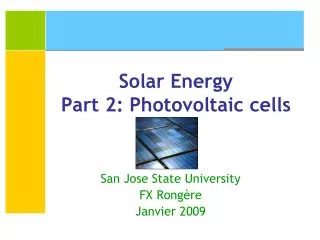
Solar Energy Part 2: Photovoltaic cells. San Jose State University FX Rongère Janvier 2009. Photovoltaic effect. Discovered by Edmond Bequerel in 1839 First Solar cell was built by Charles Fritts in 1883 Russel Ohl patented the first modern solar cell in 1946

E N D
Solar EnergyPart 2: Photovoltaic cells San Jose State University FX Rongère Janvier 2009
Photovoltaic effect • Discovered by Edmond Bequerel in 1839 • First Solar cell was built by Charles Fritts in 1883 • Russel Ohl patented the first modern solar cell in 1946 • Bell Laboratories found that doped silicon may have high photovoltaic properties in 1954
Photovoltaic Effect • Photovolatic effect is generated when • Photons hit a semi-conductor material • With a higher energy than the gap between its Valence and Conduction bands • Free electrons move on one side (n-side) while holes move on the other side (p-side) • A difference of potential is created between n-side and p-side allowing current through a load outside of the semi-conductor
Silicon based photovoltaic cells • Silicon is a metalloid of the Group IV and Period 3 • It has 14 electrons on 3 orbits (2,8,4) • Its crystalline structure is Face-centered Cubic; each Si atom is surrounded by four other atoms • Every atom of the Valence band is bonded with one atom of a neighbor saturating the valence band
Silicon based photovoltaic cells • Its band gap (at 300 K) is 1.2 eV • Doping with Boron and Phosphor dramatically improves its photovoltaic properties Charge Carriers Silicon has 4 variance electrons Phosphore has 5 variance electrons Boron has 3 variance electrons
Silicon based photovoltaic cells • N-P Jonction P N Electron diffusion Hole diffusion + + + - - - P N Electric Field
Effective radiation on solar cell • Minimum photon energy is required to move an electron from valence to conduction (band gap) Conduction + heat Valence Electron Transmission Conduction + heat Valence Electron Thermalization
Effective radiation on silicon based cells Solar Spectral Irradiance (103 W.m-2.μm) λ (m) Conversion No conversion
The Shockley-Queisser limit • The Shockley-Queisser limit is a measure of the upper obtainable conversion rate of a perfect solar cell based on only one solar cell material with only one electronic band gap • Conversion rate of a perfect Si based cell is 33% • Thermalization: 47% • Transmission: 18% • Recombination: 1.5%
Structure of a silicon Solar Cell contacts N-layer N-P junction P-layer Amp. Maximum Power Short circuit current E=0.5 Volt, 3 Amp. (typically) Volts Open circuit voltage
Manufacturing (1,900 oC) Siemens Source: Renewable Energy, Power for a sustainable future. G. Boyle, 2004
Manufacturing (1) • Silicon is obtained from Silica (SiO2) • Carbothermic reduction: • Temperature 1,900oC • Reaction with charcoal • Bulk silicon is already doped with p-type (boron) (2.1016 atoms/cm3) (Silicon: 5.1022 atoms/cm3) • Bulk silicon is sliced in 180-350 μm wafers Czochralski process
Czochralski process • Procedures: • High-purity, semiconductor-grade silicon (only a few parts per million of impurities) is melted down in a crucible (1,500 oC) • A seed crystal, mounted on a rod, is dipped into the molten silicon • The seed crystal’s rod is pulled upwards and rotated at the same time • Precise control of temperature gradients, rate of pulling and speed of rotation, it is possible to extract a large, single-crystal, cylindrical ingot from the melt. • Inert atmosphere, such as argon
Si based Solar cells • Mono-crystalline Solar cell • Conversion rate (panel): 15-20% • Major Manufacturers: SunPower, SunTech, Sharp • 35% of the market • Poly-crystalline Solar cell • Conversion rate (panel): 11-15% • Major Manufacturers: Kyocera, Sharps, Q-cell, SunTech, BP Solar, Photowatt • 60% of the market
Energy for silicon based solar panels • About 2,000 to 5,000 MJ/m2 (2005) leading to an energy payback of 1.5 to 2.5 years. Source: M. Asema, M. de Wild-Scholten THE REAL ENVIRONMENTAL IMPACTS OF CRYSTALLINE SILICON PV MODULES: AN ANALYSIS BASED ON UP-TO-DATE MANUFACTURERS DATA
Manufacturing (2) Source: Renewable Energy, Power for a sustainable future. G. Boyle, 2004
Manufacturing (2) • N-type elements (Phosphor) are injected by surface diffusion (1019 atoms/cm3) • Anti-reflection 100+ nm coating with silicon nitride deposited by PECVD • Electrodes are then put in place: • In the back aluminum base layer on the all surface • On the front silver base layer with “fingers” and “bus-bars” in order to reduce the shaded area on the cells
Manufacturing (3) • Coating to reduce the absorption of the photons by the cell • Silicon reflectance: 40% • Film treatment reduces it to 3% Active Source: Chelikowsky, J. R. and M. L. Cohen, Phys. Rev. B14, 2 (1976) 556-582.
Glass Coating • Transmittance enhancement vu
Minimal thickness of silicon cell • Absorption coefficient iλ: Light intensity x: depth aλ: Absorption coefficient Active Jellison, Jr., G. E. and F. A. Modine, Appl. Phys. Lett- 41, 2 (1982) 180-182.
Minimal thickness of silicon cell • Theoretically, 1-3 mm of bulk silicon would be needed to absorb photons • Practically, rays are reflected by a layer of aluminum on the back of the cell and trapped in the layer of silicon by texturing the upper surface • Typically, silicon solar cell wafer are 200-300 μm thick
Module Conversion rates • Electrical efficiency and module optimization increase overall conversion rate Nota: CZ-Si: mono-Si MC-Si: multi-Si Source: B. von Roedern and H.S. UllalThe Role of Polycrystalline Thin-Film PV Technologies in Competitive PV Module Markets. NREL 33rd IEEE Photovoltaic Specialists Conference San Diego, California May 11–16, 2008
Silicon Manufacturing Capacity • Worldwide evolution of the capacity of major manufacturers
Other cell technologies • First generation: bulk silicon • Mono-crystalline silicon multi-junctions • Mono-crystalline silicon • Multi-crystalline silicon • Second generation: thin films • a-Si:H amorphous hydrogenated silicon • CIGS Copper-Indium-Gallium-Selenium • CuInxGa(1-x)Se2 (x є [0,1]) • Band gap = fct(x) є [1.0μm,1.7μm]) • CdTe Cadmium Tellerium
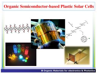
Other Technologies • 3rd generation: Non semi-conductor based • Dye cells: photo-electrochemical cells • OPV: Organic polymers • Nanocrystal • 4th generation: Composite technologies
GaAs Multijunction • Capture more solar radiation bandwidth by combining semi-conductors with different band gaps • GaAs Gallium Arsenide • Band gap: 1.43 eV • λ=.87 μm • Ge Germanium • band gap: 0.67 eV • λ=1.85 μm • InGaP Indium Gallium Phosphide • Band gap: 2.26 eV • λ=.55 μm InGaP GaAs Ge GaAs crystal
Solfocus • Started in 2005 at PARC in Palo Alto • Received $150M in VC funding
Amorphous Silicon a-Si:H • Mainly used for small devices like calculators • Si atoms are not arranged in an organized crystal • Some atoms are partially not bonded to others • Hydrogen atoms are used to fill the defects • May be degraded by high energy light Source: DOE
Ga/(Ga+In) =(1-x) 0.3 0.6 0.9 18 16 Efficiency (%) 14 12 10 1.0 1.1 1.2 1.3 1.4 1.5 1.6 CIGS • Copper Indium Gallium Selenium • Solid solution of copper indium selenide ("CIS") and copper gallium selenide, • Chemical formula of CuInxGa(1-x)Se2 Best efficiency for 1-x=.31 Absorber band gap (μm) Source: Rommel NoufiHigh Efficiency CdTe and CIGS Thin Film Solar Cells: Highlights of the Technologies Challenges NREL 2007
CIGS • Cell structure [n] ZnO, ITO2500 Å CdS700 Å [p] CIGS1-2.5 µm Mo0.5-1 µm Glass,Metal Foil,Plastics Source: Rommel NoufiHigh Efficiency CdTe and CIGS Thin Film Solar Cells: Highlights of the Technologies Challenges NREL 2007
CdTe • Cadmium Telluride – Cadmium Sulfide • Band Gap: 1.5 eV • Cell structure CdS [n] ZnTe :Cu [p] CdTe CdS ZnTe :Cu 2µm
Thin-film Companies Source: H.S. Ullal and B. von Roedern Thin Film CIGS and CdTe Photovoltaic Technologies: Commercialization, Critical Issues, and Applications NREL 2007
Applications • CdTe panels in Walpolentz (Germany) 40 MW
Applications • GIGS panels in Wales (84 kW)
Technology Comparison Source: Navigant Photovoltaic Manufacturer Shipments & Competitive Analysis 2006/2007 April 2007
Solar cost • Solar module Source: http://www.solarbuzz.com/
Solar Cost • Example of cost split • Today, installed cost is $7-$10/Wp Source: Meng TAO Inorganic Photovoltaic Solar Cells: Silicon and Beyond The Electrochemical Society Interface • Winter 2008
Cost reduction • First Solar (CdTe) cost reduction road map Source: First Solar Corporate Overview Q3 2008
Module Conversion Rates • California Solar Initiative recommendation Source: CSI - List of Eligible Inverters http://www.gosolarcalifornia.org/csi/step3.html
Photovoltaics • System Off grid Grid-tied
Inverter • Converts DC in AC by a commutation device • Issues are: • Harmonics • Failure of the switching device • Efficiency 90%-95% • Cost: $1/W Ex: Xantrex GT 3.0 Inverter
Inverter Efficiencies • California Solar Initiative recommendations Source: CSI - List of Eligible Inverters http://www.gosolarcalifornia.org/equipment/inverter.php
Some PV companies • Information: • www.solarbuzz.com • Distributors: • www.sunwize.com • Local companies to follow • www.Appliedmaterials.com • www.Miasole.com • www.Calisolar.com • www.solyndra.com • www.Nanosolar.com • www.Sunpowercorp.com • www.Akeena.com • www.EnergyInnovations.com • www.Nanosysinc.com • www.solfocus.com Solfocus PV concentrator