DIGITAL CIRCUITS
DIGITAL CIRCUITS. Dr. L M Head Sophomore Clinic Fall 2004. Decimal. Binary. 0. 0000. 1. 0001. 2. 0010. 7 0111 - 5 0101 2 0010 5 0101 - 2 0010 3 0011. 2 0010 +5 0101 7 0111 3 0011 +5 0101 8 1000. 3.


DIGITAL CIRCUITS
E N D
Presentation Transcript
DIGITAL CIRCUITS Dr. L M Head Sophomore Clinic Fall 2004
Decimal Binary 0 0000 1 0001 2 0010 7 0111 - 5 0101 2 0010 5 0101 - 2 0010 3 0011 2 0010 +5 0101 7 0111 3 0011 +5 0101 8 1000 3 0011 4 0100 5 0101 6 0110 7 0111 8 1000 9 1001 Binary Numbers and Boolean Logic http://www.neurophys.wisc.edu/www/comp/docs/ascii.html
Binary Designations As seen in the above example, the four digit binary representation of the number 5 is 0101. Binary numbers are read from right to left, and the total is the sum of all individual digits represented by a “1”. For “5”, the third or “4” digit is added to the first or “1” digit, bringing the total to five.
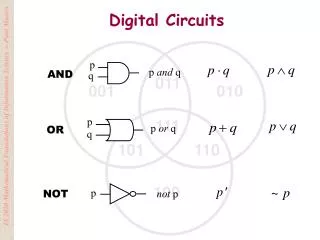
AND Gate symbol • The AND gate implements the AND function. With the gate shown above, both inputs must have logic 1 (high) signals applied to them in order for the output to be logic 1. With either input at logic 0 (low), the output will be held to logic 0. The AND Gate is not limited to only two inputs. AND Gates are also commonly manufactured to have three or four inputs.
OR Gate symbol + The OR gate is sort of the reverse of the AND gate. The OR function, like its verbal counterpart, allows the output to be true (logic 1) if any one or more of its inputs are true. Verbally, we might say, "If it is raining OR if I turn on the sprinkler, the lawn will be wet." Note that the lawn will still be wet if the sprinkler is on and it is also raining. This is correctly reflected by the basic OR function.
Inverter symbols ‾ or ~Otherwise known as a NOT Gate The inverter is a little different from AND and OR gates in that it always has exactly one input as well as one output. Whatever logical state is applied to the input, the opposite state will appear at the output. For example, if a logic 0 is applied to the input, the output would be a logic 1. In the inverter symbol, the triangle actually denotes only an amplifier, which in digital terms means that it "cleans up" the signal but does not change its logical sense. It is the circle at the output, which denotes the logical inversion. The circle could have been placed at the input instead, and the logical meaning would still be the same. For shorthand, the inverter may simply be shown as the circle.
NAND Gate = The NAND gate implements the NAND function, which is exactly inverted from the AND function you already examined. With the gate shown above, both inputs must have logic 1 signals applied to them in order for the output to be a logic 0. With either input at logic 0, the output will be held to logic 1. The circle at the output of the NAND gate denotes the logical inversion, just as it did at the output of the inverter. Also in the figure above, note that the overbar is a solid bar over both input values at once. This shows that it is the AND function itself that is inverted, rather than each separate input.
NOR Gate = The NOR gate is an OR gate with the output inverted. Where the OR gate allows the output to be true (logic 1) if any one or more of its inputs are true, the NOR gate inverts this and forces the output to logic 0 when any input is true. In symbols, the NOR function is designated with a plus sign (+), with an overbar over the entire expression to indicate the inversion. In logical diagrams, the symbol above designates the NOR gate. As expected, this is an OR gate with a circle to designate the inversion.
XOR GateOtherwise known as the Exclusive-OR The Exclusive-OR, or XOR function is an interesting and useful variation on the basic OR function. Verbally, it can be stated as, "Either A or B, but not both." The XOR gate produces a logic 1 output only if its two inputs are different. If the inputs are the same, the output is a logic 0. The XOR symbol is a variation on the standard OR symbol. It consists of a plus (+) sign with a circle around it. The logic symbol, as shown here, is a variation on the standard OR symbol.
F = (A•B) • (C•D) Implementing a Function Find F if A=1 B=0 C=0 D=1 F = (A•B) + (C•D)
LM555 Timer 74LS90 Binary Counter SCHS086 Decoder Seven-Segment Display The Digital Timer The timer/clock is a standard LM555 astable oscillator configuration with external components to set the frequency. The 74LS90 Binary Counter counts the pulses from the LM555 timer and turns those pulses into the “4-bit” output. Each decimal digit has its own binary code of ones and zeros. The counter tells the SCHS086 Decoder which sections of the seven-segment display to light up to show the proper number. So when the counter outputs 0001, the decoder will tell the two vertical right hand segments of the display to light up.
RA RB Frequency = ((1.44)/(RA +2RB)C) The LM555 is an IC device that can generate a time signal usually referred to as an oscillation. Timing is an essential part of most electronic devices. For the most part, timing is used to set which pins in the chip will go on at any given time. In order to do this the chip must be connected first to an input voltage, then through a series of resistors and capacitors. These resistors, connected to the threshold and discharge pins, as well as the capacitor, connected to the trigger pin, will decide what frequency the timer will operate at.
14 13 12 11 10 9 8 1 2 3 4 5 6 7 To 555 Timer DM74LS90 COUNTER A D TO GROUND 6V B C TO GROUND The input counts pulses generated by the LM555 timer chip and the outputs are as described in the appropriate truth table. The connections designated A, B, C, and D connect to the inputs of the BCD to seven-segment decoder. To Decoder
6V 16 15 14 13 12 11 10 9 1 2 3 4 5 6 7 8 6V f g e d c b a MC 14543B BCD C B D A 6V TO GROUND 470 ohm 470 ohm 470 ohm 470 ohm 470 ohm 470 ohm 470 ohm The Decoder will be, in a sense, “told” from the decade counter which sections of the seven-segment display to light up. For example, if the counter outputs 0001, the decoder will tell the two vertical right hand segments of the display to light up. From Counter To 7-segment Display
The display component is a common-anode seven-segment display. The chip is composed of seven light emitting diodes (LEDs) combined to make the number display. This chip takes the information being sent from the decoder and lights up the corresponding number with the LEDs. A combination of the LEDs is turned on or off to make the appropriate number.