Optimizing Data Transmission in FPGA Sequencing Process
This document discusses optimizing data transmission from FEPGA to SEQPGA, focusing on data serialization, control words, ADC bits, and card upgrades. It explores methods to improve trigger calculations and fiber link cost management. Includes detailed schemes, illustrations, and examples.

Optimizing Data Transmission in FPGA Sequencing Process
E N D
Presentation Transcript
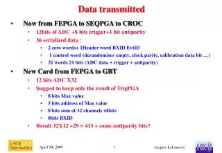
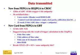
Data transmitted • Now from FEPGA to SEQPGA to CROC • 12bits of ADC +8 bits trigger+1 bit antiparity • 36 serialized data : • 2 zero words+ 1Header word BXID EvtID • 1 control word (derandomiser empty, clock parity, calibration data bit …) • 32 words 21 bits (ADC data + trigger + antiparity) • New Card from FEPGA to GBT • 12 bits ADC X32 • Suggest to keep only the result of trigger calculation in the TrigPGA • 8 bits Max value • 5 bits address of Max value • 8 bits sum of 32 channels x8bits • 8bits BXID • Result 32X12 +29 = 413 + some antiparity bits? Jacques Lefrancois
Cost vs number of optical fiber link • 200 euros per fiber link • A Tell 40 evaluation is 20Keuros for about 100-120 fibers from J-P Cachemiche • http://indico.cern.ch/getFile.py/access?contribId=6&resId=0&materialId=slides&confId=48992 • Electronic upgrade meeting February 2nd 2009 • Optimistic? • Total cost about 400 euros /fiber • If enough fibers and enough data in one Tell40, could one do 2D zero suppress in Tell 40: 2 crates => about 28 cards =>84-112 fibers??? Jacques Lefrancois
Packing in Tell1 Jacques Lefrancois
Present Decision 4-12 bits in Tell1 • Part of packing is for trigger data dropped in the upgrade. • Before packing average ADC value is 256.5 • If the ADC value is between 248 and 263 =>subtract 248 and get 4bit value • Otherwise give original 12bits Jacques Lefrancois
Scheme without compression • 384 +29 bits minimum =413 need more than 5X80 need 6 fibers =>480bits • Use extra space for Card and crate address+Fiber address + antiparity? =10 bits • Use BXID in each Fiber? Use crate and Fiber address in each Fiber? Antiparity in each Fiber? Jacques Lefrancois
Data to be sent • For reason of architecture simplification and to keep reserve data throughput possibility => decide to have 4 Fibers one fiber (80 bits dat) per FPGA of 8 channels • In each fibers some fixed data for each beam crossing • 6 bits of trigger information (1/4 of full trigger info) =>8? • BXID info 8 bits? • 8 bits pattern of 4bits or 12bits ADC data for example: 11000010 • 8 times 4bits of ADC data => 32bits (it may become 40 bits if we decide to switch short ADC to long ADC at 5bits instead of 4) • Depending on event from 0 x8bits to 8X8bits for long ADC data • Total data length from 56 to 120 or 64 to 128: data has to be organised by bytes Jacques Lefrancois
Sequential Scheme • In a sequential scheme (a la Tell1) one could send successive event of variable length in the GBT • if all data is in miniblocks of 8bits as it seemed in the previous slide one could have 8FIFO but each would nevertheless have to work at 16X 40MHz =640MHz to build up from 128 bit string to 80bit every 25ns • This is unreasonable for ProAsic 3E or 3L whose RAM seems limited to 250MHz • However with some multiplexing it might become feasible =see transparency 13 and after Jacques Lefrancois
Fixed format scheme • Another possibility is to prepare data in a quasi fixed format 80 bits wide in FPGA dual port RAM • Because of some needed manipulation one has to alternate between two such RAM 256 bits deep (it should be enough to derandomize, if needed could go to 512) • Part of the Data has a fixed format • 6bits trigger +1 : FPGA +card+crate address, +1: data quality (i.e. no overflow) • Since the address is fixed it can be 1 bit wide and n-bit deep • 8bits BXID • 8bits map of 4(or5) bits and full 12bits ADC • 8X4 or 8X5 low value ADC content 32 or 40 • This takes 64 out of 80 bits available each 25ns • Use the 16 bits left to write two 8 bits ADC data If more data are to be written one uses more lines. If less data less lines Jacques Lefrancois
Example of 4 first lines out of 256 address data quality trigger BXID short data map long data 1bit 1bit 6bits 8bits 40 bits 8 bits 8bits + 8bits 1 0 110001 00000000 01…101.. 00000000 0101011101001100 1 0 001101 00000001 00….11… 01000000 10001110 00100111 0 0 010001 00000010 10….01…. 00110010 00011100 11100000 0 0 000011 00000011 000…11… 11000110 11100011 01110101 The colour indicates which long data is coming from which event. From the map it is easy to reconstruct which long data comes from which ADC of which event As long as there are less than 512 long data in 256 events with 8 ADC there is no overflow. (Seems OK: Monte CARLO test ongoing) If the sum of the map bits at 1 reaches 512 before the end of the 256 samples the data quality bit is put at one indicating overflow until the end of the 256 lines. Jacques Lefrancois
How to write the long data • One uses the fact that dual port RAMs in FPGA can be written and read in different format • For each 25ns sample one writes the 64 bits, corresponding to the fixed format, in a RAM 256 deep (4 X 4096 bits blocks) • One writes in a RAM 8X8bits wide and 256 deep the 8 possible long ADC data some of these (the ones corresponding to 0 in the map) will contain meaningless data or better 0 • This RAM will be read as 8bits wide and 2K deep some of the address will correspond to meaningless data • Simultaneously one builds from the map data a table of pointer of up to 512 possible address of meaningful data (11 bits address from 0 to 2047). This pointer table can be considered as a FIFO memory of the pointer address up to 512 deep Jacques Lefrancois
The pointer FIFO and the readout • Because the pointer FIFO is up to 512 deep and not 256 it has to be built and used at 80MHz which is not a problem in the ProAsic3 or the AX500 • To be safe from timing conflict it is needed to alternate between two RAM systems every 256 X25ns => no problem each system needs only 9 blocks of 4Kbit RAM • One start to read the 8 bits-map RAM at the start of the cycle if there is 0 in the map this is done one line/25 ns if there are 1's in the map the FIFO has to be written and the next readout can be delayed by up to 8X12.5ns (perhaps 6X12.5ns). The worse case is 192 lines of 00000000 followed by 64 lines of 11111111. The writing of the FIFO is finished 192+256 clock cycles after the start < 512. 512 is the time allowed since there are two alternate system • The read-out on the GBT starts 256 cycle after initial read-in and ends 512 cycles after Jacques Lefrancois
Conclusion on fixed format • A " fixed format scheme" can be implemented to compress data without requiring clock cycle faster than 80MHz • The scheme implies some desynchronisation of "long ADC" data up to 256 clock cycle . However it has the advantage that the data in all fibers all cards and all crates are synchronized which can be useful in simplifying event building in the TELL40 • Further saving => 3 fibers/card would probably not have enough bandwith and it is very ackward to go from 4FPGA to 3Fibers Jacques Lefrancois
Sequential: the organisation • As mentioned before the needed frequency to manipulate bytes is too fast to directly use the FPGA RAMS • A way out is to quadruple the system writing in turn in 4 memory systems, storing 256 events in each system. The available time to do byte manipulation on 256 events in one system is then 256X4X25ns = 25.6microsecond • A first memory 128 bits or 16 bytes long 256 deep (8 blocks) is used to store incoming data (data is defined as the previous 128 bit string of transparency 9) THIS IS CALLED RAM1 • RAM1 is rotated to become 8 blocks of 1 bit wide 4096 deep. At a given address of the 8 blocks the 8bits are one of the original bytes. The 16 bytes of an event are at successive address. • RAM2 will be the target RAM it has 5 blocks of 8 wide (the bytes) and 512 deep. It will be read at 80 MHz to form 10 X 8bits every 25ns in the GBT during 256 clock cycles. Jacques Lefrancois
The transfer • RAM1 consist of successive 16 bytes. The first 8 are the fixed data which have to be transferred. The next 8 are long ADC some of which will be a byte with 8 zero's. These 0 should not be transferred. • Reading RAM1 at 160MHz one can go thru the full 4096 in the allowed 25.6 microsec. The bytes are written in RAM2, cycling thru the 5 blocks with multiplexer and then thru the address. It is like a IJ address I from 0-511 J from 0 to 4. If a line of 0 is detected when reading RAM1 (among the 8 long ADC) no writing in RAM2 is done and the IJ counter is not incremented • At the end we have packed data in RAM2. What is not elegant is that most of the time the packed data is << than 256X80 the last part is irrelevant but will be transmitted. It would have been easier to debug if irrelevant data would be put to zero! (discussed at the end of next slide) Jacques Lefrancois
The readout in the GBT • One cannot write the data before it is produced. but the last value of the packed data can be transferred from RAM1 25600ns after the start. So the start of the readout could be before this 25600ns but by a time which cannot be more than the time needed to write the minimum data in the GBT . The minimum data is 256x8 bytes =2048 bytes Since we write 10bytes/25ns =5.12 microsec so the data is delayed by about 20-21 microsec • Since new data will not arrive before 25.6 microsec there is time I believe to write zeros in the second half of RAM2 (this takes 3.2 microsec) ahead of the arrival of the next group of 256 events Jacques Lefrancois
A variant • We know from the 12bit BXID which bunches has no collisions • We could decide that all the 16 bytes of an event for such BXID are not written in RAM2 • There are at least 33 such empty BXID out of a group of 256 events. This saves us at least space for an extra 33X8=264 bytes, compared to the 512 usually available for long ADC bytes. • The first or the last 80 bits word of a group of 256 should be reserved for a header or trailer of information :total 12bit BXID FPGA,CARD,CRATE address. BXID number after which there is an overflow etc… The way to do this in the complicated timing has not been worked out yet. Jacques Lefrancois
Conclusion on sequential method:Pro and Cons • A possible way to do sequential readout has been found • It request 4X(8+5) blocks =52 while a A3PE1500 has 60. We need 6 blocks for test RAM 256 deep 8X12 bits wide =>58! • The Pro of the method is that the data is in a format which is probably more natural for computer treatment=> less treatment in the TELL40. The pro is also that with the variant it allows more fat event without overflow. • The Con is that the data arrives with a larger delay than with the first method. How do we recognize in the TELL40 that we start a new group of 256 since the BXID information is not in a fixed position. The Con is also that we stretch the use of the A3PE1500 in memory (58 blocks) and in frequency 160MHz and perhaps in combinatorial cells to have these 4 independent processing systems. Jacques Lefrancois